Fairchild NC7SV17 TinyLogic ULP- A Single Buffer with Schmitt Trigger Input Data Manual
Summary
Enhance your low-voltage designs with the NC7SV17 single buffer. This ultra-low power device incorporates a Schmitt trigger input and operates efficiently across an extended range from 0.9V to 3.6V, making it ideal for battery-powered or space-constrained high-speed electronics. It provides reliable signal conditioning while maintaining exceptional energy efficiency using advanced CMOS technology. The accompanying documentation is a complete technical guide, offering detailed specifications on operating ranges (Absolute Maximum Ratings), pin configurations (SC70/MicroPak), and performance graphs to ensure optimal system integration for professional engineers.
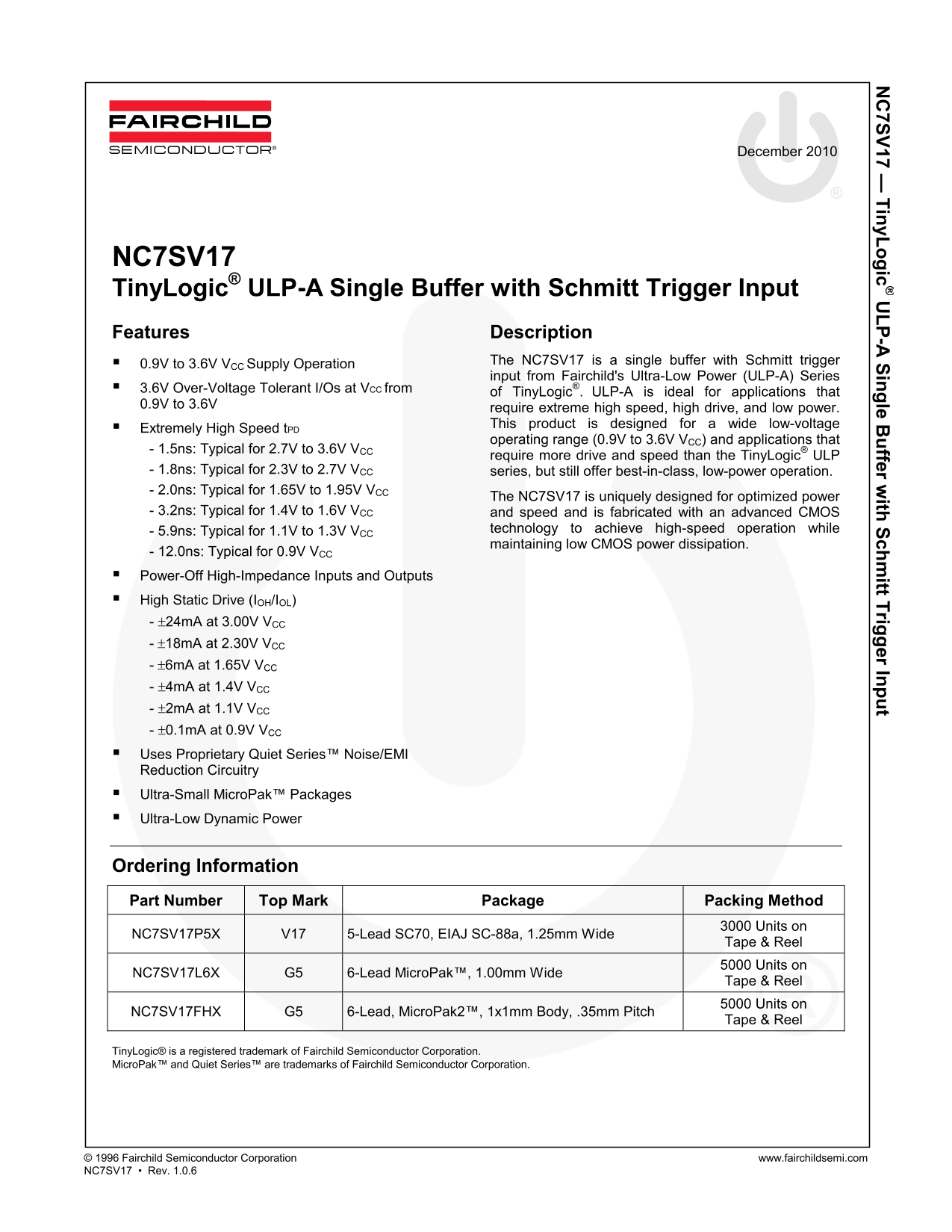
Page 1 Text Content
7SV17 — Tiny Logic LP-A Single B uffer w ith Schm itt Trigger Input
December 2010
NC7SV17 Tiny Logic® ULP-A Single Buffer with Schmitt Trigger Input Features Description
0.9V to 3.6V VCC Supply Operation The NC7SV17 is a single buffer with Schmitt trigger input from Fairchild's Ultra-Low Power (ULP-A) Series
3.6V Over-Voltage Tolerant I/Os at VCC from
of Tiny Logic®. ULP-A is ideal for applications that
0.9V to 3.6V
require extreme high speed, high drive, and low power. This product is designed for a wide low-voltage
Extremely High Speed t PD
operating range (0.9V to 3.6V VCC) and applications that
- 1.5ns: Typical for 2.7V to 3.6V VCC
require more drive and speed than the Tiny Logic® ULP
- 1.8ns: Typical for 2.3V to 2.7V VCC series, but still offer best-in-class, low-power operation. - 2.0ns: Typical for 1.65V to 1.95V VCC
The NC7SV17 is uniquely designed for optimized power
- 3.2ns: Typical for 1.4V to 1.6V VCC and speed and is fabricated with an advanced CMOS
- 5.9ns: Typical for 1.1V to 1.3V VCC technology to achieve high-speed operation while maintaining low CMOS power dissipation.
- 12.0ns: Typical for 0.9V VCC Power-Off High-Impedance Inputs and Outputs High Static Drive (IOH/IOL) - ±24m A at 3.00V VCC - ±18m A at 2.30V VCC - ±6m A at 1.65V VCC - ±4m A at 1.4V VCC - ±2m A at 1.1V VCC - ±0.1m A at 0.9V VCC Uses Proprietary Quiet Series™ Noise/EMI Reduction Circuitry Ultra-Small Micro Pak™ Packages Ultra-Low Dynamic Power
Ordering Information Part Number Top Mark Package Packing Method
NC7SV17P5X V17 5-Lead SC70, EIAJ SC-88a, 1.25mm Wide 3000 Units on
Tape & Reel
NC7SV17L6X G5 6-Lead Micro Pak™, 1.00mm Wide 5000 Units on
Tape & Reel
NC7SV17FHX G5 6-Lead, Micro Pak2™, 1x1mm Body, .35mm Pitch 5000 Units on
Tape & Reel
Tiny Logic® is a registered trademark of Fairchild Semiconductor Corporation. Micro Pak™ and Quiet Series™ are trademarks of Fairchild Semiconductor Corporation.
© 1996 Fairchild Semiconductor Corporation www.fairchildsemi.com NC7SV17 • Rev. 1.0.6
Page Summary Contents For Fairchild NC7SV17 TinyLogic ULP- A Single Buffer with Schmitt Trigger Input Data Manual
Manual Details
| Brand | Fairchild |
|---|---|
| Pages | 11 |
| File Size | 547.25 KB |
| Published | July 22, 2026 |
Enter the captcha to get the download link:
