FAIRCHILD FSTD16861 20-Bit Bus Switch with Level Shifting Data Manual
Summary
This technical manual provides comprehensive details for the FSTD16861, a 20-bit bus switch designed for CMOS TTL applications requiring level shifting. It enables reliable signal switching between high-voltage (5V) inputs and lower-voltage (3.3V) outputs. The document covers deep operational specifications, including electrical characteristics, absolute maximum ratings, pin descriptions, and circuit diagrams. This resource is essential for electronics engineers and hardware designers utilizing sophisticated bus connectivity in integrated systems.
Page 1 Text Content
16861 20-B it B s S itch ith evel S iftin
May 2001 Revised June 2005
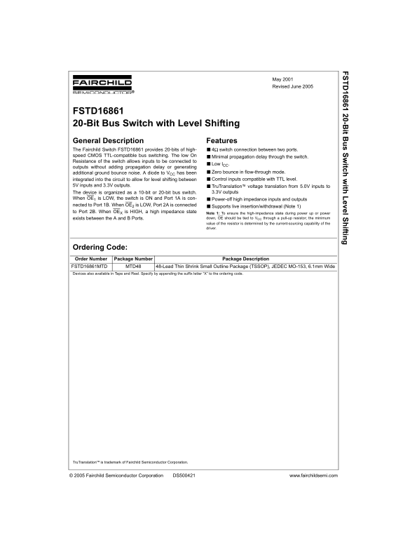
FSTD16861 20-Bit Bus Switch with Level Shifting General Description Features The Fairchild Switch FSTD16861 provides 20-bits of high- ■4: switch connection between two ports. speed CMOS TTL-compatible bus switching. The low On
■Minimal propagation delay through the switch.
Resistance of the switch allows inputs to be connected to
■Low l CC.
outputs without adding propagation delay or generating
additional ground bounce noise. A diode to VCC has been ■Zero bounce in flow-through mode. integrated into the circuit to allow for level shifting between ■Control inputs compatible with TTL level.
5V inputs and 3.3V outputs. ■Tru Translation¥ voltage translation from 5.0V inputs to
The device is organized as a 10-bit or 20-bit bus switch. 3.3V outputs
When OE1 is LOW, the switch is ON and Port 1A is con- ■Power-off high impedance inputs and outputs nected to Port 1B. When OE2 is LOW, Port 2A is connected
■Supports live insertion/withdrawal (Note 1)
to Port 2B. When OEX is HIGH, a high impedance state Note 1: To ensure the high-impedance state during power up or power
exists between the A and B Ports. down, OE should be tied to VCC through a pull-up resistor; the minimum value of the resistor is determined by the current-sourcing capability of the driver.
Ordering Code: Order Number Package Number Package Description FSTD16861MTD MTD48 48-Lead Thin Shrink Small Outline Package (TSSOP), JEDEC MO-153, 6.1mm Wide Devices also available in Tape and Reel. Specify by appending the suffix letter “X” to the ordering code.
Tru Translation¥ is trademark of Fairchild Semiconductor Corporation.
© 2005 Fairchild Semiconductor Corporation DS500421 www.fairchildsemi.com
Page Summary Contents For FAIRCHILD FSTD16861 20-Bit Bus Switch with Level Shifting Data Manual
Manual Details
| Brand | Fairchild |
|---|---|
| Pages | 6 |
| File Size | 172.52 KB |
| Published | June 06, 2026 |
Enter the captcha to get the download link:

Frequently Asked Questions
What type of logic levels does this switch support?
It supports CMOS TTL-compatible switching and includes a diode for level shifting from 5V inputs to 3.3V outputs.
Are there restrictions on the input voltage?
The recommended operating input voltage range is 0V to 5.5V DC.
How is the high impedance state achieved during power cycling?
To ensure a high-impedance state during power up or power down, OE should be tied to V through a pull-up resistor.
What is the On Resistance of the switch?
The typical On Resistance (R_ON) is 4.7 Ohm at 25°C when applying voltage across the A and B ports.