Fairchild FDMF6705B User Guide
Summary
This advanced DrMOS module provides a high-performance, ultra-compact power stage solution for demanding DC-DC conversion applications. Integrating MOSFETs, driver ICs, and a Schottky diode into an extra-small package (6x6mm), it achieves over 93% efficiency and handles up to 40A with minimal ringing. The comprehensive manual covers technical specifications, detailed application circuits, pin definitions, and physical dimensions required for seamless implementation in high-performance computing environments, including gaming motherboards, data center servers, and workstations needing robust power management.
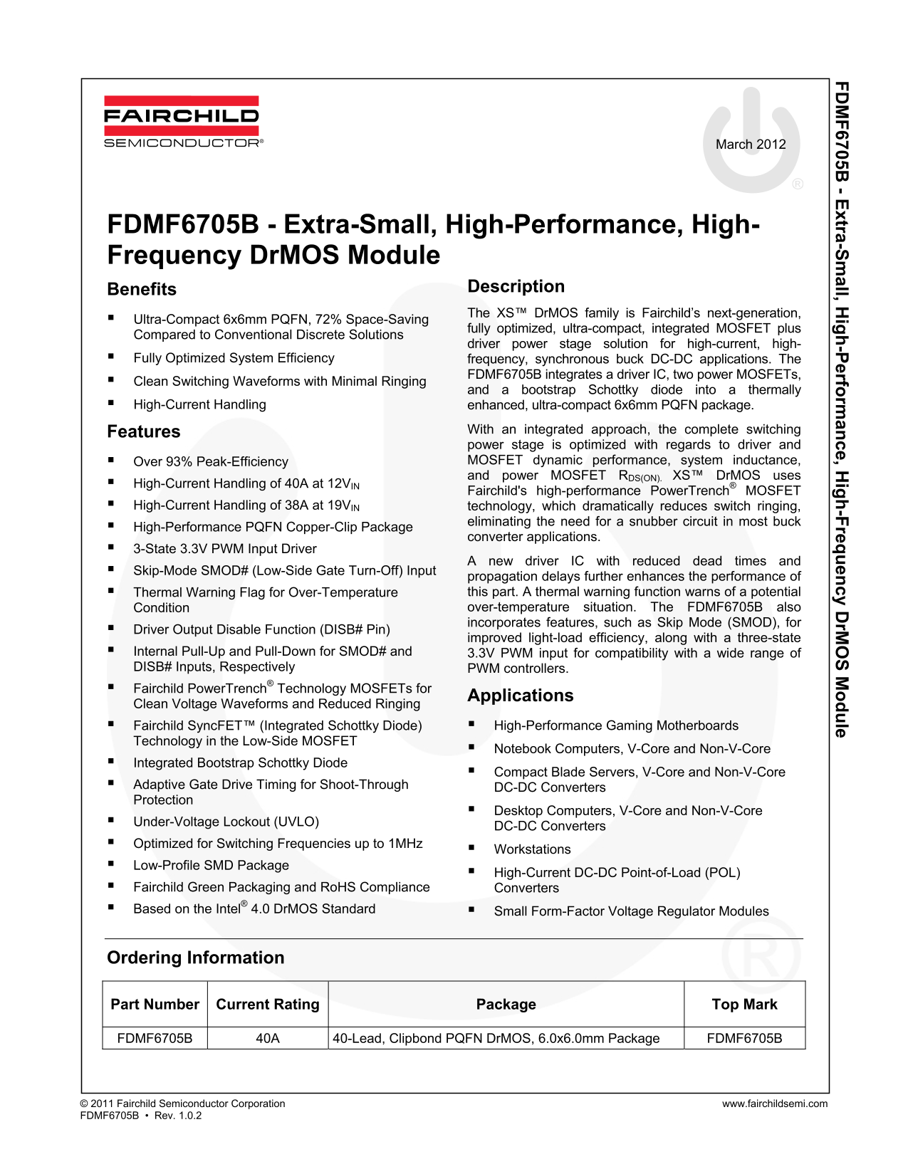
Page 1 Text Content
6705B - E xtra-S all, H ig -P erfo rm an ce, H ig -F req en cy D r M le
March 2012
FDMF6705B - Extra-Small, High-Performance, High- Frequency Dr MOS Module
Benefits Description The XS™ Dr MOS family is Fairchild’s next-generation,
Ultra-Compact 6x6mm PQFN, 72% Space-Saving
fully optimized, ultra-compact, integrated MOSFET plus
Compared to Conventional Discrete Solutions
driver power stage solution for high-current, high-
Fully Optimized System Efficiency frequency, synchronous buck DC-DC applications. The
FDMF6705B integrates a driver IC, two power MOSFETs,
Clean Switching Waveforms with Minimal Ringing
and a bootstrap Schottky diode into a thermally
High-Current Handling enhanced, ultra-compact 6x6mm PQFN package.
Features With an integrated approach, the complete switching power stage is optimized with regards to driver and Over 93% Peak-Efficiency MOSFET dynamic performance, system inductance, and power MOSFET RDS(ON). XS™ Dr MOS uses
High-Current Handling of 40A at 12VIN
Fairchild's high-performance Power Trench® MOSFET
High-Current Handling of 38A at 19VIN technology, which dramatically reduces switch ringing,
eliminating the need for a snubber circuit in most buck
High-Performance PQFN Copper-Clip Package
converter applications.
3-State 3.3V PWM Input Driver
A new driver IC with reduced dead times and
Skip-Mode SMOD# (Low-Side Gate Turn-Off) Input
propagation delays further enhances the performance of Thermal Warning Flag for Over-Temperature this part. A thermal warning function warns of a potential Condition over-temperature situation. The FDMF6705B also incorporates features, such as Skip Mode (SMOD), for
Driver Output Disable Function (DISB# Pin)
improved light-load efficiency, along with a three-state
Internal Pull-Up and Pull-Down for SMOD# and 3.3V PWM input for compatibility with a wide range of DISB# Inputs, Respectively PWM controllers. Fairchild Power Trench® Technology MOSFETs for
Applications
Clean Voltage Waveforms and Reduced Ringing
Fairchild Sync FET™ (Integrated Schottky Diode) High-Performance Gaming Motherboards
Technology in the Low-Side MOSFET
Notebook Computers, V-Core and Non-V-Core
Integrated Bootstrap Schottky Diode
Compact Blade Servers, V-Core and Non-V-Core
Adaptive Gate Drive Timing for Shoot-Through DC-DC Converters Protection
Desktop Computers, V-Core and Non-V-Core
Under-Voltage Lockout (UVLO)
DC-DC Converters
Optimized for Switching Frequencies up to 1MHz
Workstations
Low-Profile SMD Package
High-Current DC-DC Point-of-Load (POL)
Fairchild Green Packaging and Ro HS Compliance Converters Based on the Intel® 4.0 Dr MOS Standard Small Form-Factor Voltage Regulator Modules
Ordering Information
Part Number Current Rating Package Top Mark
FDMF6705B 40A 40-Lead, Clipbond PQFN Dr MOS, 6.0x6.0mm Package FDMF6705B
© 2011 Fairchild Semiconductor Corporation www.fairchildsemi.com FDMF6705B • Rev. 1.0.2
Page Summary Contents For Fairchild FDMF6705B User Guide
Manual Details
| Brand | Fairchild |
|---|---|
| Pages | 19 |
| File Size | 1.47 MB |
| Published | July 06, 2026 |
Enter the captcha to get the download link:

Frequently Asked Questions
What is the core advantage of the XS™ DrMOS family compared to traditional solutions?
It offers an ultra-compact, fully optimized integrated MOSFET plus driver power stage solution, improving efficiency and size.
How high are the peak efficiencies achievable with this module?
The module achieves over 93% Peak-Efficiency due to its optimized design and advanced technology.
What features help reduce switching ringing and simplify circuit design?
It uses Fairchild PowerTrench MOSFETs, which significantly reduces switch ringing, often eliminating the need for a snubber circuit in buck converters.
What does the Thermal Warning Flag function do?
The thermal warning function alerts users to a potential over-temperature situation during operation.