Fairchild FDB035N10A User Guide
Summary
This high-performance N-Channel PowerTrench MOSFET is engineered for demanding power switching applications, featuring extremely low on-state resistance and fast switching speeds up to 214A. The comprehensive manual provides critical technical details, including maximum electrical ratings, thermal characteristics, and performance curves required for design integration. It is specifically recommended for professional engineers designing DC/DC Converters, Server/Telecom PSUs, Uninterruptible Power Supplies (UPS), battery chargers, and AC motor drives needing reliable high-current handling.
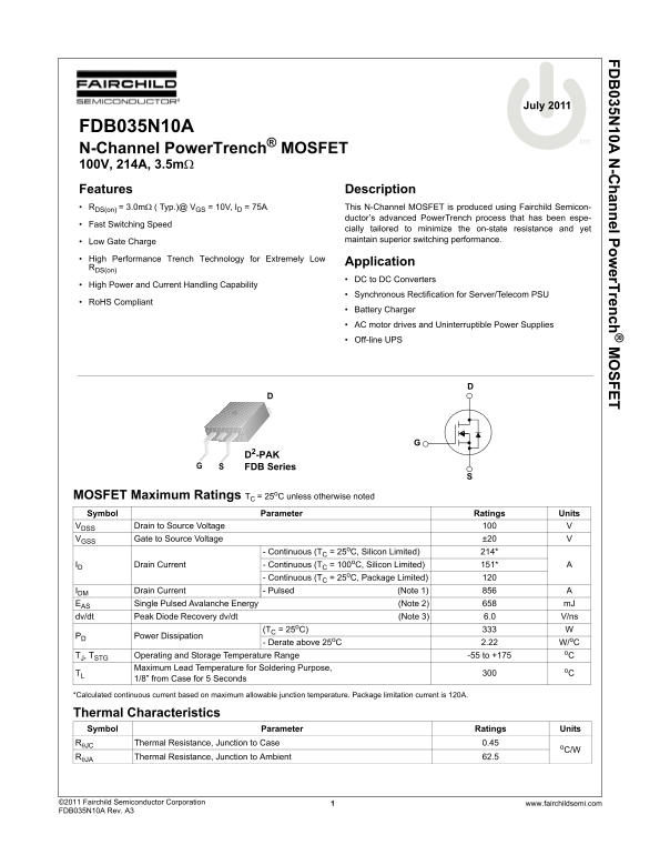
Page 1 Text Content
FD 035N 10A -C hannel Pow er Trench SFET
July 2011
FDB035N10A
N-Channel Power Trench® MOSFET 100V, 214A, 3.5mΩ Features Description RDS(on) = 3.0mΩ ( Typ.)@ VGS = 10V, ID = 75A This N-Channel MOSFET is produced using Fairchild Semicon-
ductor’s advanced Power Trench process that has been espe-
Fast Switching Speed
cially tailored to minimize the on-state resistance and yet Low Gate Charge maintain superior switching performance.
High Performance Trench Technology for Extremely Low
Application
RDS(on)
DC to DC Converters
High Power and Current Handling Capability
Synchronous Rectification for Server/Telecom PSU
Ro HS Compliant
Battery Charger
AC motor drives and Uninterruptible Power Supplies Off-line UPS
D2-PAK FDB Series G
MOSFET Maximum Ratings TC = 25o C unless otherwise noted Symbol Parameter Ratings Units
VDSS Drain to Source Voltage VGSS Gate to Source Voltage ±20
- Continuous (TC = 25o C, Silicon Limited) 214*
ID Drain Current 151* A- Continuous (TC = 100o C, Silicon Limited)
- Continuous (TC = 25o C, Package Limited)
IDM Drain Current - Pulsed (Note 1) EAS Single Pulsed Avalanche Energy (Note 2) m J
dv/dt Peak Diode Recovery dv/dt (Note 3) 6.0 V/ns
(TC = 25o C)
PD Power Dissipation
- Derate above 25o C 2.22 W/o C
TJ, TSTG Operating and Storage Temperature Range -55 to +175 Maximum Lead Temperature for Soldering Purpose, o C
1/8” from Case for 5 Seconds
*Calculated continuous current based on maximum allowable junction temperature. Package limitation current is 120A.
Thermal Characteristics Symbol Parameter Ratings Units
RθJC Thermal Resistance, Junction to Case 0.45
RθJA Thermal Resistance, Junction to Ambient 62.5
©2011 Fairchild Semiconductor Corporation www.fairchildsemi.com1 FDB035N10A Rev. A3
Page Summary Contents For Fairchild FDB035N10A User Guide
Manual Details
| Brand | Fairchild |
|---|---|
| Pages | 9 |
| File Size | 262.32 KB |
| Published | May 20, 2026 |
Enter the captcha to get the download link:

Frequently Asked Questions
What is the nominal static drain-to-source on resistance (Rds(on))?
The typical Rds(on) is 3.0 mΩ at V = 10V and I = 75A.
What are the maximum continuous current ratings for this device?
Drain Current can be 214 A continuously (T=25C) or 151 A continuously (T=100C).
What voltage range is suitable for mounting the MOSFET?
The specified Drain to Source Voltage (VDS) rating is up to 100 V.
Is this component compatible with high-power applications?
Yes, it offers high power and current handling capability and is RoHS Compliant.