Fairchild FDD86110 User Guide
Summary
This advanced N-Channel Power Trench MOSFET is a high-efficiency semiconductor component designed for demanding power electronics applications, such as DC-DC Conversion systems. Engineered to minimize on-state resistance while maintaining superior switching performance, it boosts system reliability and efficiency. The accompanying manual provides comprehensive technical details, covering electrical characteristics, thermal management guidelines, and application ratings necessary for professional engineers and designers building robust power conversion circuits.
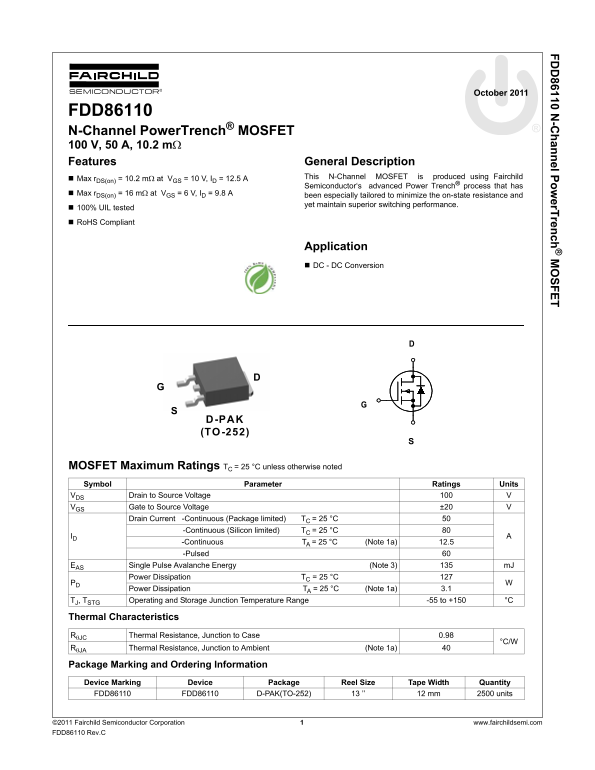
Page 1 Text Content
FD 86110 N -C hannel Pow er Trench SFET
October 2011
FDD86110 N-Channel Power Trench® MOSFET 100 V, 50 A, 10.2 mΩ Features General Description
This N-Channel MOSFET is produced using Fairchild
Max r DS(on) = 10.2 mΩ at VGS = 10 V, ID = 12.5 A
Semiconductor‘s advanced Power Trench® process that has
Max r DS(on) = 16 mΩ at VGS = 6 V, ID = 9.8 A
been especially tailored to minimize the on-state resistance and yet maintain superior switching performance.
100% UIL tested
Ro HS Compliant
Application DC - DC Conversion
TO -252D-PAK (TO-252)
MOSFET Maximum Ratings TC = 25 °C unless otherwise noted Symbol Parameter Ratings Units
VDS Drain to Source Voltage VGS Gate to Source Voltage ±20 Drain Current -Continuous (Package limited) TC = 25 °C 50 -Continuous (Silicon limited) TC = 25 °C
-Continuous TA = 25 °C (Note 1a) 12.5
-Pulsed EAS Single Pulse Avalanche Energy (Note 3) m J Power Dissipation TC = 25 °C
Power Dissipation TA = 25 °C (Note 1a) 3.1
TJ, TSTG Operating and Storage Junction Temperature Range -55 to +150 °C
Thermal Characteristics
RθJC Thermal Resistance, Junction to Case 0.98
RθJA Thermal Resistance, Junction to Ambient (Note 1a)
Package Marking and Ordering Information Device Marking Device Package Reel Size Tape Width Quantity FDD86110 FDD86110 D-PAK(TO-252) 13 ’’ 12 mm 2500 units
©2 011 Fairchild Semiconductor Corporation 1 www.fairchildsemi.com FD D86110 Rev.C
Page Summary Contents For Fairchild FDD86110 User Guide
Manual Details
| Brand | Fairchild |
|---|---|
| Pages | 6 |
| File Size | 252.18 KB |
| Published | May 31, 2026 |
Enter the captcha to get the download link:

Frequently Asked Questions
What is the maximum continuous drain current (ID) rating?
The Drain Current can be up to 12.5 A continuously, limited by the silicon.
Are these parts counterfeit-resistant?
Fairchild encourages purchasing parts directly or from Authorized Fairchild Distributors for guaranteed genuine components and traceability.