FAIRCHILD BS270 User Guide
Summary
This manual covers the BS270 N-Channel MOSFET, a 60V, 400mA enhancement mode field-effect transistor designed for low-voltage switching applications. It is ideal for controlling small servo motors and driving power MOSFET gates, featuring low on-state resistance and rugged reliability.
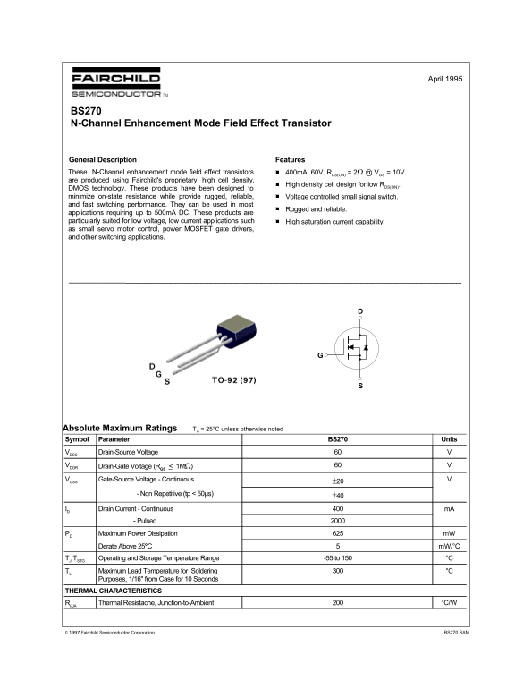
Page 1 Text Content
April 1995
BS270 N-Channel Enhancement Mode Field Effect Transistor
General Description Features These N-Channel enhancement mode field effect transistors 400m A, 60V. RDS(ON) = 2Ω @ VGS = 10V. are produced using Fairchild's proprietary, high cell density,
High density cell design for low RDS(ON).
DMOS technology. These products have been designed to minimize on-state resistance while provide rugged, reliable, Voltage controlled small signal switch. and fast switching performance. They can be used in most
Rugged and reliable.
applications requiring up to 500m A DC. These products are particularly suited for low voltage, low current applications such High saturation current capability. as small servo motor control, power MOSFET gate drivers, and other switching applications.
Absolute Maximum Ratings TA = 25°C unless otherwise noted Symbol Parameter BS270 Units VDSS Drain-Source Voltage
VDGR Drain-Gate Voltage (RGS < 1MΩ)
VGSS Gate-Source Voltage - Continuous ±20
- Non Repetitive (tp < 50µs) ±40
ID Drain Current - Continuous 400 m A
- Pulsed
PD Maximum Power Dissipation m W
Derate Above 25°C m W/°C
TJ,TSTG Operating and Storage Temperature Range -55 to 150 °C
TL Maximum Lead Temperature for Soldering °C Purposes, 1/16" from Case for 10 Seconds
THERMAL CHARACTERISTICS
RθJA Thermal Resistacne, Junction-to-Ambient °C/W
© 1997 Fairchild Semiconductor Corporation BS270.SAM
Page Summary Contents For FAIRCHILD BS270 User Guide
Manual Details
| Brand | Fairchild |
|---|---|
| Pages | 10 |
| File Size | 339.18 KB |
| Published | June 15, 2026 |
Enter the captcha to get the download link:

Frequently Asked Questions
Max drain-source voltage?
60V.
Max continuous drain current?
400 mA.
On-resistance at V_GS=10V?
2 ohms max.
Authorized for life support?
No, requires express approval.
Typical applications?
Small servo motor control, MOSFET gate drivers, low current switching.