Fairchild FDMF6704A User Guide
Summary
This ultra-compact DrMOS module is a next-generation solution for designing high-frequency, high-current synchronous buck DC-DC converters. Featuring integrated MOSFETs, driver ICs, and advanced protection circuits in an energy-efficient 6mm x 6mm package, it delivers optimized power conversion with minimal parasitics. The manual provides comprehensive technical details on the module's application circuit, pin configuration, and system integration guidelines. It is ideal for electrical engineers designing robust voltage regulation solutions for demanding platforms such as blade servers, desktop computers, workstations, and networking equipment.
Page 1 Text Content
FD F6704A The X tra S all, H igh P erform ance, H igh Frequency D r M odule
August 2009
FDMF6704A - XSTM Dr MOS
The Xtra Small, High Performance, High Frequency Dr MOS Module Benefits General Description Ultra compact size - 6 mm x 6 mm MLP, 44 % space The XSTM Dr MOS family is Fairchild’s next-generation fully- saving compared to conventional MLP 8 mm x 8 mm optimized, ultra-compact, integrated MOSFET plus driver power Dr MOS packages. stage solutions for high current, high frequency synchronous
buck DC-DC applications. The FDMF6704A XSTM Dr MOS
Fully optimized system efficiency.
integrates a driver IC, two power MOSFETs and a bootstrap
Clean voltage waveforms with reduced ringing.
Schottky diode into a thermally enhanced, ultra compact 6 mm x
High frequency operation.
6 mm MLP package. With an integrated approach, the complete switching power stage is optimized with regards to driver and
Features
MOSFET dynamic performance, system inductance and RDS(ON). This greatly reduces the package parasitics and layout
Ultra- compact thermally enhanced 6 mm x 6 mm MLP
challenges associated with conventional discrete solutions.
package 84 % smaller than conventional discrete solutions.
XSTM Dr MOS uses Fairchild's high performance
Synchronous driver plus FET multichip module.
Power Trench TM 5 MOSFET technology, which dramatically
High current handling of 35 A.
reduces ringing in synchronous buck converter applications.
Over 93 % peak efficiency. Power Trench TM 5 can eliminate the need for a snubber circuit in
Logic level PWM input. buck converter applications. The driver IC incorporates advanced features such as SMOD for improved light load
Fairchild's Power Trench® 5 technology MOSFETs for clean
efficiency. A 5 V gate drive and an improved PCB interface
voltage waveforms and reduced ringing.
optimized for a maximum low side FET exposed pad area,
Optimized for high switching frequencies of up to 1 MHz.
ensure higher performance. This product is compatible with
Skip mode SMOD [low side gate turn off] input.
the new Intel 6 mm x 6 mm Dr MOS specification.
Fairchild Sync FETTM [integrated Schottky diode] technology
in the low side MOSFET. Applications
Integrated bootstrap Schottky diode. Compact blade servers V-core, non V-core and VTT DC-DC
converters.
Adaptive gate drive timing for shoot-through protection.
Desktop computers V-core, non V-core and VTT DC-DC
Driver output disable function [DISB# pin].
converters.
Undervoltage lockout (UVLO).
Workstations V-core, non V-core and VTT DC-DC
Fairchild Green Packaging and Ro HS
converters.
compliant. Low profile SMD package.
Gaming Motherboards V-core, non V-core and VTT DC-DC converters. Gaming consoles. High-current DC-DC Point of Load (POL) converters. Networking and telecom microprocessor voltage regulators. Small form factor voltage regulator modules.
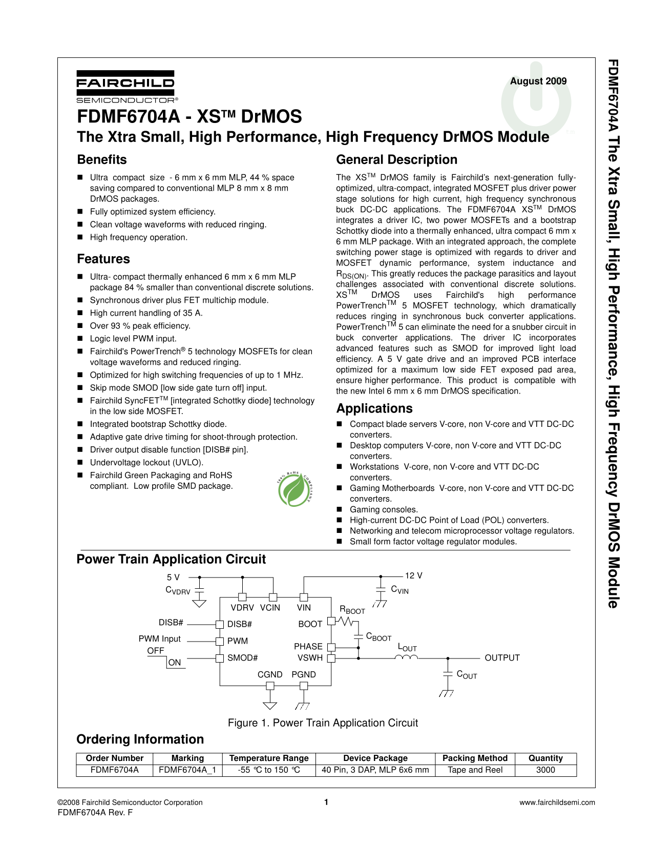
Power Train Application Circuit
5 V 12 V CVDRV CVIN
VDRV VCIN VIN RBOOT
DISB# DISB# BOOT
CBOOT
PWM Input
PHASE LOUT
SMOD#ON VSWH OUTPUT
CGND PGND COUT
Figure 1. Power Train Application Circuit
Ordering Information Order Number Marking Temperature Range Device Package Packing Method Quantity FDMF6704A FDMF6704A_1 -55 °C to 150 °C 40 Pin, 3 DAP, MLP 6x6 mm Tape and Reel
©2008 Fairchild Semiconductor Corporation www.fairchildsemi.com FDMF6704A Rev. F
Page Summary Contents For Fairchild FDMF6704A User Guide
Manual Details
| Brand | Fairchild |
|---|---|
| Pages | 14 |
| File Size | 715.41 KB |
| Published | July 15, 2026 |
Enter the captcha to get the download link:
