Fairchild FDD8876 FDU8876 User's Manual
Summary
A high-performance N-Channel PowerTrench MOSFET optimized for efficiency in demanding electrical systems. This component is designed for modern DC/DC converters that utilize synchronous or conventional PWM switching, offering extremely low on-resistance and fast switching speed. The comprehensive datasheet provides essential technical specifications, including maximum ratings, detailed electrical curves, thermal performance graphs, and guidelines for high power and current handling across various mounting packages (e.g., D-PAK TO-252). It is essential inventory for electronics engineers developing advanced, reliable power conversion solutions.
Page 1 Text Content
April 2008
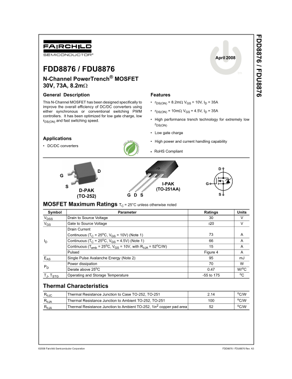
FDD8876 / FDU8876
N-Channel Power Trench® MOSFET 30V, 73A, 8.2mΩ General Description Features This N-Channel MOSFET has been designed specifically to r DS(ON) = 8.2mΩ, VGS = 10V, ID = 35A improve the overall efficiency of DC/DC converters using
either synchronous or conventional switching PWM r DS(ON) = 10mΩ, VGS = 4.5V, ID = 35A
controllers. It has been optimized for low gate charge, low
High performance trench technology for extremely low
r DS(ON) and fast switching speed.
r DS(ON)
Low gate charge
Applications
High power and current handling capability
DC/DC converters
• Ro HS Compliant
I-PAK (TO-251AA)
TO-252D-PAK
(TO-252)
MOSFET Maximum Ratings TC = 25°C unless otherwise noted Symbol Parameter Ratings Units VDSS Drain to Source Voltage VGS Gate to Source Voltage ±20
Drain Current
AContinuous (TC = 25o C, VGS = 10V) (Note 1)
ID Continuous (TC = 25o C, VGS = 4.5V) (Note 1)
Continuous (Tamb = 25o C, VGS = 10V, with RθJA = 52o C/W) Pulsed Figure 4
EAS Single Pulse Avalanche Energy (Note 2) m J
Power dissipation
Derate above 25o C 0.47 W/o C
TJ, TSTG Operating and Storage Temperature -55 to 175
Thermal Characteristics
RθJC Thermal Resistance Junction to Case TO-252, TO-251 2.14
RθJA Thermal Resistance Junction to Ambient TO-252, TO-251
RθJA Thermal Resistance Junction to Ambient TO-252, 1in2 copper pad area
2008 Fairchild Semiconductor Corporation FDD8876 / FDU8876 Rev. A3
Page Summary Contents For Fairchild FDD8876 FDU8876 User's Manual
Manual Details
| Brand | Fairchild |
|---|---|
| Pages | 11 |
| File Size | 468.42 KB |
| Published | May 28, 2026 |
Enter the captcha to get the download link:

Frequently Asked Questions
What is the maximum continuous drain current at 25°C?
The maximum continuous drain current (ID) listed is 73 A.
What specific applications was this MOSFET designed for?
It is optimized for DC/DC converters and high power, current handling capability.
Can I use these components in life support systems?
No, the products are not authorized for use as critical components in life support devices without express written approval.