Fairchild FDD86102 User Guide
Summary
Discover the FDD86102 N-Channel PowerTrench MOSFET, an advanced semiconductor component optimized for high-efficiency power applications like DC-DC conversion. Featuring ultra-low on-resistance and fast switching characteristics, this surface-mount MOSFET handles high current (36A) within a compact package. This technical manual provides comprehensive engineering data, covering maximum ratings, detailed electrical parameters, thermal profiles, and dynamic switching curves essential for electrical engineers designing reliable power electronics systems.
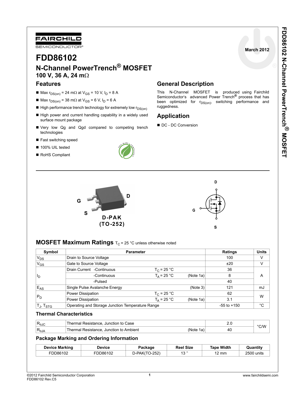
Page 1 Text Content
FD 86102 N -C hannel Pow er Trench SFET
March 2012
FDD86102 N-Channel Power Trench® MOSFET 100 V, 36 A, 24 mΩ Features General Description
Max r DS(on) = 24 mΩ at VGS = 10 V, ID = 8 A This N-Channel MOSFET is produced using Fairchild Semiconductor‘s advanced Power Trench® process that has
Max r DS(on) = 38 mΩ at VGS = 6 V, ID = 6 A
been optimized for r DS(on), switching performance and ruggedness.
High performance trench technology for extremely low r DS(on)
High power and current handling capability in a widely used
Application
surface mount package
DC - DC Conversion
Very low Qg and Qgd compared to competing trench technologies
Fast switching speed
100% UIL tested
Ro HS Compliant
TO -252D-PAK (TO-252)
MOSFET Maximum Ratings TC = 25 °C unless otherwise noted Symbol Parameter Ratings Units VDS Drain to Source Voltage
VGS Gate to Source Voltage ±20 Drain Current -Continuous TC = 25 °C 36
ID A -Continuous TA = 25 °C (Note 1a)
-Pulsed EAS Single Pulse Avalanche Energy (Note 3) m J Power Dissipation TC = 25 °C 62
Power Dissipation TA = 25 °C (Note 1a) 3.1
TJ, TSTG Operating and Storage Junction Temperature Range -55 to +150 °C
Thermal Characteristics
RθJC Thermal Resistance, Junction to Case 2.0
RθJA Thermal Resistance, Junction to Ambient (Note 1a)
Package Marking and Ordering Information Device Marking Device Package Reel Size Tape Width Quantity FDD86102 FDD86102 D-PAK(TO-252) 13 ’’ 12 mm 2500 units
©20 12 Fairchild Semiconductor Corporation www.fairchildsemi.com1 FD D86102 Rev.C5
Page Summary Contents For Fairchild FDD86102 User Guide
Manual Details
| Brand | Fairchild |
|---|---|
| Pages | 6 |
| File Size | 390.79 KB |
| Published | July 15, 2026 |
Enter the captcha to get the download link:

Frequently Asked Questions
What is the continuous drain current capability of the MOSFET?
The device has a maximum continuous drain current (ID) rating of 36 A at room temperature (T = 25 °C).
How does mounting configuration affect heat dissipation?
Thermal resistance (R) will be significantly lower when mounted on a two-ounce copper pad compared to an area-array connection.
What is the guaranteed maximum drain-source on-resistance (RDS(on))?
The specified typical RDS(on) at V = 6 V, I = 6 A is 38 mΩ.
Is this MOSFET suitable for DC-DC conversion circuits?
Yes, the general features list indicates that surface mount packages are optimized for use in DC - DC Conversion applications.