Fairchild FDD306P User's Manual
Summary
This low-resistance P-Channel MOSFET is engineered with advanced PowerTrench technology for superior performance in battery power management circuits. Designed specifically for applications such as DC/DC converters, it provides fast switching speed and high current handling capability. The accompanying manual offers comprehensive technical specifications, including detailed electrical characteristics, thermal ratings, on-resistance data, and operational guidelines essential for reliable circuit design by electronics engineers.
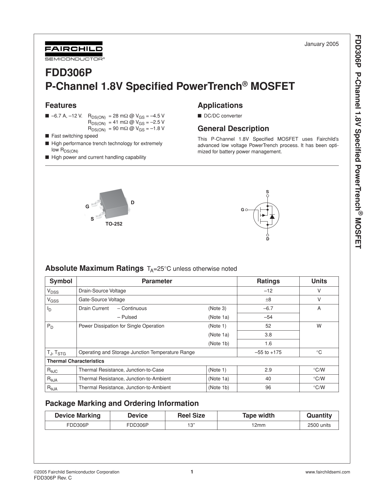
Page 1 Text Content
306P -C an el 1.8V ecifi ed er Tren ch
January 2005
FDD306P P-Channel 1.8V Specified Power Trench MOSFET Features Applications –6.7 A, –12 V. DS(ON) = 28 m @ V GS = –4.5 V DC/DC converter
DS(ON) = 41 m @ V GS = –2.5 V DS(ON) = 90 m @ V GS = –1.8 V General Description
Fast switching speed
This P-Channel 1.8V Specified MOSFET uses Fairchild’s
High performance trench technology for extremely
advanced low voltage Power Trench process. It has been opti-
low R DS(ON)
mized for battery power management.
High power and current handling capability
TO-252
Absolute Maximum Ratings =25°C unless otherwise noted Symbol Parameter Ratings Units
Drain-Source Voltage –12
Gate-Source Voltage
Drain Current – Continuous (Note 3) –6.7
– Pulsed (Note 1a) –54
Power Dissipation for Single Operation (Note 1)
(Note 1a) 3.8 (Note 1b) 1.6
, T Operating and Storage Junction Temperature Range –55 to +175 STG Thermal Characteristics
Thermal Resistance, Junction-to-Case (Note 1) 2.9 C/W
Thermal Resistance, Junction-to-Ambient (Note 1a) C/W
Thermal Resistance, Junction-to-Ambient (Note 1b) C/W
Package Marking and Ordering Information Device Marking Device Reel Size Tape width Quantity FDD306P FDD306P 13’’ 12mm 2500 units
©2005 Fairchild Semiconductor Corporation www.fairchildsemi.com FDD306P Rev. C
Page Summary Contents For Fairchild FDD306P User's Manual
Manual Details
| Brand | Fairchild |
|---|---|
| Pages | 5 |
| File Size | 505.64 KB |
| Published | July 12, 2026 |
Enter the captcha to get the download link:

Frequently Asked Questions
What is the typical on-resistance of the MOSFET?
At -2.5 V and a drain current of -6.7 A, the R_DS(ON) is 41 mΩ.
Are there restrictions on using this component in life support systems?
Yes, it requires express written approval from Fairchild Semiconductor Corporation.
What are the maximum allowable voltages for this transistor?
The max Drain-Source Voltage is –12 V, and the Gate-Source Voltage can be ±8V.