Fairchild FDC658P User's Manual
Summary
Fairchild FDC658P is a P-channel PowerTrench MOSFET with -30V rating, 0.050 ohm Rds(on), and 8nC gate charge. Available in SuperSOT-6 (72% smaller than SO-8), SOT-23, SOIC-16, SOT-223, and SO-8 packages. Targets notebook and portable electronics designers for load switching, battery charging, and DC-DC conversion applications.
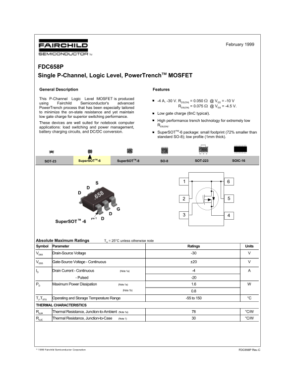
Page 1 Text Content
February 1999
FDC658P Single P-Channel, Logic Level, Power Trench TM MOSFET
General Description Features
This P-Channel Logic Level MOSFET is produced
-4 A, -30 V. RDS(ON) = 0.050 Ω @ VGS = -10 V
using Fairchild Semiconductor's advanced
RDS(ON) = 0.075 Ω @ VGS = -4.5 V.
Power Trench process that has been especially tailored to minimize the on-state resistance and yet maintain
Low gate charge (8n C typical).
low gate charge for superior switching performance.
High performance trench technology for extremely low
These devices are well suited for notebook computer
RDS(ON).
applications: load switching and power management, battery charging circuits, and DC/DC conversion. Super SOTTM-6 package: small footprint (72% smaller than
standard SO-8); low profile (1mm thick).
Super SOTTM-8 SO-8 SOT-223Super SOTTM-6 SOIC-16SOT-23
Super SOT -6TM
Absolute Maximum Ratings TA = 25°C unless otherwise note Symbol Parameter Ratings Units
VDSS Drain-Source Voltage -30
VGSS Gate-Source Voltage - Continuous ±20
ID Drain Current - Continuous (Note 1a) -4
- Pulsed -20
PD Maximum Power Dissipation (Note 1a) 1.6
(Note 1b)
TJ,TSTG Operating and Storage Temperature Range -55 to 150 °C THERMAL CHARACTERISTICS RθJA Thermal Resistance, Junction-to-Ambient (Note 1a) °C/W RθJC Thermal Resistance, Junction-to-Case (Note 1) °C/W
© 1999 Fairchild Semiconductor Corporation FDC658P Rev.C
Page Summary Contents For Fairchild FDC658P User's Manual
Manual Details
| Brand | Fairchild |
|---|---|
| Pages | 5 |
| File Size | 106.87 KB |
| Published | June 17, 2026 |
Enter the captcha to get the download link:

Frequently Asked Questions
What is the maximum drain-source voltage of the FDC658P?
The maximum drain-source voltage is -30V.
What are typical applications for this MOSFET?
It is suited for load switching, power management, and battery charging circuits in notebook computers.
What is the typical total gate charge?
The typical total gate charge is 12nC at VGS = -4.5V and ID = -15A.
Can this MOSFET be used in life support devices?
No, it is not authorized for use as a critical component in life support devices without written approval.