Fairchild FDC6561AN User's Manual
Summary
The DC6561AN is a high-performance Logic Level N-Channel MOSFET designed using advanced PowerTrench technology. Featuring exceptional low on-state resistance and rapid switching capabilities, this device is ideal for efficient power management solutions in battery-powered systems. This technical manual provides comprehensive electrical characteristics, thermal ratings (including $R_{\theta JC}$), operating guidelines, and detailed parameters necessary for electronics engineers to successfully design and implement optimal switching circuits.
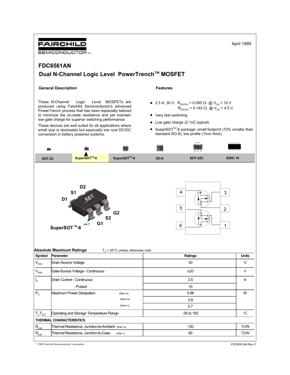
Page 1 Text Content
April 1999
FDC6561AN Dual N-Channel Logic Level Power Trench TM MOSFET
General Description Features
These N-Channel Logic Level MOSFETs are
2.5 A, 30 V. RDS(ON) = 0.095 Ω @ VGS = 10 V
produced using Fairchild Semiconductor's advanced
RDS(ON) = 0.145 Ω @ VGS = 4.5 V
Power Trench process that has been especially tailored to minimize the on-state resistance and yet maintain Very fast switching. low gate charge for superior switching performance.
Low gate charge (2.1n C typical).
These devices are well suited for all applications where
small size is desireable but especially low cost DC/DC Super SOTTM-6 package: small footprint (72% smaller than conversion in battery powered systems. standard SO-8); low profile (1mm thick).
Super SOTTM-8 SO-8 SOT-223Super SOTTM-6 SOIC-16SOT-23
pin G1
Super SOT -6TM
Absolute Maximum Ratings TA = 25°C unless otherwise note Symbol Parameter Ratings Units
VDSS Drain-Source Voltage
VGSS Gate-Source Voltage - Continuous ±20
ID Drain Current - Continuous 2.5
- Pulsed 10
PD Maximum Power Dissipation (Note 1a) 0.96
(Note 1b)
(Note 1c)
TJ,TSTG Operating and Storage Temperature Range -55 to 150 °C THERMAL CHARACTERISTICS RθJA Thermal Resistance, Junction-to-Ambient (Note 1a) °C/W RθJC Thermal Resistance, Junction-to-Case (Note 1) °C/W
© 1999 Fairchild Semiconductor Corporation FDC6561AN Rev.C
Page Summary Contents For Fairchild FDC6561AN User's Manual
Manual Details
| Brand | Fairchild |
|---|---|
| Pages | 5 |
| File Size | 114.20 KB |
| Published | June 18, 2026 |
Enter the captcha to get the download link:

Frequently Asked Questions
What operating temperature range can this device handle?
The operating and storage temperature range is -55 °C to 150 °C.
How small are the gate charge characteristics?
It features a low gate charge (2.1nC typical), which ensures superior switching performance.
What kind of heat sinking setup is required for thermal management?
The case-to-ambient thermal resistance ($R_{ ext{CA}}$) uses a minimum 2oz copper pad or an exposed pad design.
Is this device suitable for low power applications?
The MOSFETs are designed to minimize on-state resistance and power dissipation rates, making them suitable for various current loads.