Fairchild FDC654P User Guide
Summary
This high-performance P-Channel Logic Level MOSFET utilizes advanced PowerTrench technology, making it ideal for efficiency-critical battery management and power conversion systems. Featuring extremely low on-resistance and optimized low gate charge, this device excels in applications such as load switches and battery protection circuits. The provided manual offers comprehensive technical specifications, detailing absolute maximum ratings, detailed electrical behaviors (On/Off characteristics), switching times, thermal analysis, and performance graphs, enabling precise design integration for robust power management solutions.
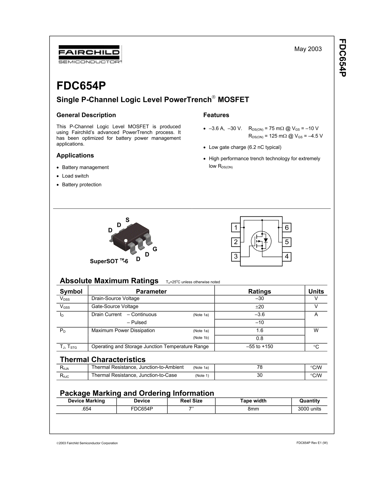
Page 1 Text Content
654P May 2003
FDC654P Single P-Channel Logic Level Power Trench MOSFET General Description Features This P-Channel Logic Level MOSFET is produced
• –3.6 A, –30 V. RDS(ON) = 75 mΩ @ VGS = –10 V
using Fairchild’s advanced Power Trench process. It
RDS(ON) = 125 mΩ @ VGS = –4.5 V
has been optimized for battery power management applications.
• Low gate charge (6.2 n C typical)
Applications
• High performance trench technology for extremely low RDS(ON)
• Battery management • Load switch • Battery protection
Super SOT -6TM
Absolute Maximum Ratings TA=25o C unless otherwise noted Symbol Parameter Ratings Units VDSS Drain-Source Voltage –30 V VGSS Gate-Source Voltage ±20 V ID Drain Current – Continuous (Note 1a) –3.6 A – Pulsed –10
Maximum Power Dissipation (Note 1a) 1.6 W PD (Note 1b) 0.8
TJ, TSTG Operating and Storage Junction Temperature Range –55 to +150 °C
Thermal Characteristics RθJA Thermal Resistance, Junction-to-Ambient (Note 1a) 78 °C/W RθJC Thermal Resistance, Junction-to-Case (Note 1) 30 °C/W
Package Marking and Ordering Information Device Marking Device Reel Size Tape width Quantity .654 FDC654P 7’’ 8mm 3000 units
2003 Fairchild Semiconductor Corporation FDC654P Rev E1 (W)
Page Summary Contents For Fairchild FDC654P User Guide
Manual Details
| Brand | Fairchild |
|---|---|
| Pages | 5 |
| File Size | 116.18 KB |
| Published | July 07, 2026 |
Enter the captcha to get the download link:

Frequently Asked Questions
What is the maximum Drain-Source Voltage (DSS) rating?
The absolute maximum drain-source voltage rating is –30 V.
Is this MOSFET suitable for battery power management?
Yes, it has been optimized for battery power management applications and low gate charge.
What is the typical on-resistance at DC when V_GS = -10V?
The typical static drain-source on-resistance (R_DS(ON)) is 75 mΩ.
How does temperature affect the on-resistance?
As junction temperature increases from –55°C to +150°C, the R_DS(ON) generally decreases in magnitude while the specified test reports show varying trends specific to operating conditions.