Fairchild FDC6333C User Guide
Summary
Experience high-performance power management with these N & P MOSFETs, engineered using advanced PowerTrench technology for superior dissipation and ultra-low on-state resistance in a compact SuperSOT-6 package. This manual is an essential technical resource for electrical engineers designing space-constrained applications such as DC/DC converters, load switches, and inverter circuits. It provides comprehensive electrical characteristics, thermal ratings, and detailed dynamic parameters for precise circuit integration.
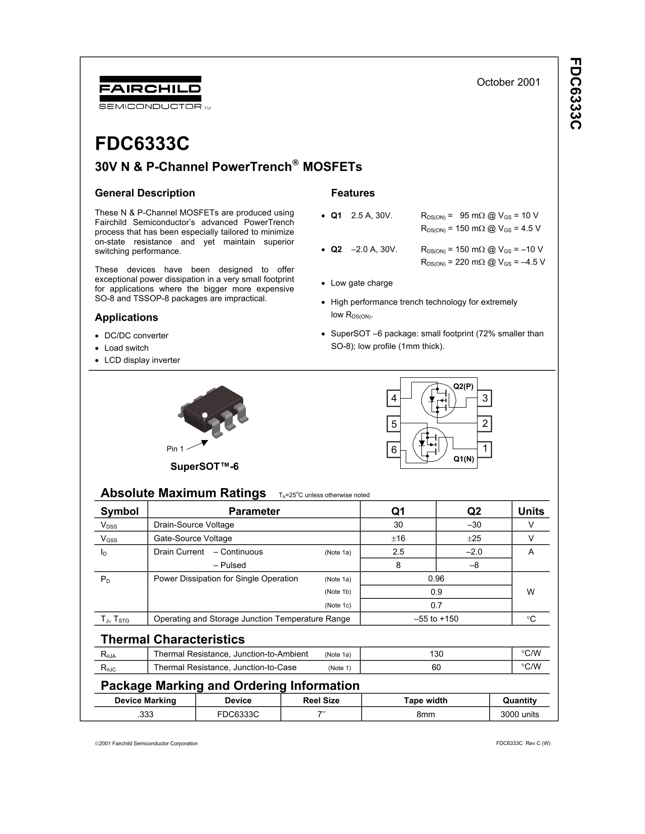
Page 1 Text Content
FD 6333C
October 2001
FDC6333C 30V N & P-Channel Power Trench MOSFETs General Description Features These N & P-Channel MOSFETs are produced using
• Q1 2.5 A, 30V. RDS(ON) = 95 mΩ @ VGS = 10 V
Fairchild Semiconductor’s advanced Power Trench
RDS(ON) = 150 mΩ @ VGS = 4.5 V
process that has been especially tailored to minimize on-state resistance and yet maintain superior
switching performance. • Q2 –2.0 A, 30V. RDS(ON) = 150 mΩ @ VGS = –10 V
RDS(ON) = 220 mΩ @ VGS = –4.5 V
These devices have been designed to offer exceptional power dissipation in a very small footprint
• Low gate charge
for applications where the bigger more expensive SO-8 and TSSOP-8 packages are impractical.
• High performance trench technology for extremely low RDS(ON).
Applications
• DC/DC converter • Super SOT –6 package: small footprint (72% smaller than • Load switch SO-8); low profile (1mm thick).
• LCD display inverter
Super SOT -6TM
Pin 1
Super SOT™-6
Absolute Maximum Ratings TA=25o C unless otherwise noted Symbol Parameter Q1 Q2 Units VDSS Drain-Source Voltage –30 VGSS Gate-Source Voltage ±16 ±25 ID Drain Current – Continuous (Note 1a) 2.5 –2.0
– Pulsed –8
PD Power Dissipation for Single Operation (Note 1a) 0.96
(Note 1b) 0.9 (Note 1c) 0.7
TJ, TSTG Operating and Storage Junction Temperature Range –55 to +150 °C
Thermal Characteristics
RθJA Thermal Resistance, Junction-to-Ambient (Note 1a) °C/W RθJC Thermal Resistance, Junction-to-Case (Note 1) °C/W
Package Marking and Ordering Information Device Marking Device Reel Size Tape width Quantity
.333 FDC6333C 7’’ 8mm 3000 units
2001 Fairchild Semiconductor Corporation FDC6333C Rev C (W)
Page Summary Contents For Fairchild FDC6333C User Guide
Manual Details
| Brand | Fairchild |
|---|---|
| Pages | 8 |
| File Size | 98.45 KB |
| Published | July 06, 2026 |
Enter the captcha to get the download link:

Frequently Asked Questions
What are the primary characteristics of the SuperSOT-6 package?
It offers a small footprint, noted as being 72% smaller than the traditional SO-8 package.
What is the operating junction temperature range for this device?
The operating and storage junction temperature range is specified from -55 to +150 J°C.
How should I calculate heat dissipation relative to ambient air?
You must consider combining the Junction-to-Case ($q_{JC}$) and Case-to-Ambient ($q_{CA}$) thermal resistances for accurate dissipation calculation.
What is the general drain current capability under certain conditions?
Under specified voltage loads, there are maximum continuous drain current ratings listed in the electrical characteristics table.