Fairchild FDC6320C User's Guide
Summary
A low-voltage, high-reliability choice for switching applications, this dual N & P channel digital FET is built with advanced DMOS technology. Ideal for modern 3V circuits and load switching, it offers excellent ESD ruggedness and can efficiently replace multiple bipolar NPN/PNP transistors. The accompanying datasheet provides comprehensive engineering details—including electrical characteristics, low on-state resistance values, and detailed switching parameters—making it an invaluable component for circuit designers needing robust performance in low power environments.
Page 1 Text Content
October 1997
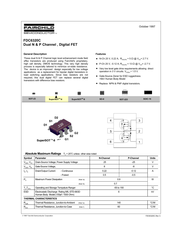
FDC6320C Dual N & P Channel , Digital FET
General Description Features These dual N & P Channel logic level enhancement mode field N-Ch 25 V, 0.22 A, RDS(ON) = 5 Ω @ VGS= 2.7 V. effec transistors are produced using Fairchild's proprietary, high cell density, DMOS technology. This very high density P-Ch 25 V, -0.12 A, RDS(ON) = 13 Ω @ VGS= -2.7 V. process is especially tailored to minimize on-state resistance.
Very low level gate drive requirements allowing direct
The device is an improved design especially for low voltage
operation in 3 V circuits. VGS(th) < 1.5 V.
applications as a replacement for bipolar digital transistors in load switching applications. Since bias resistors are not
Gate-Source Zener for ESD ruggedness.
required, this dual digital FET can replace several digital
>6k V Human Body Model
transistors with difference bias resistors.
Replace NPN & PNP digital transistors.
SOT-23 Super SOTTM-8 SOIC-16SO-8
SOT-223Super SOTTM-6
Absolute Maximum Ratings TA = 25o C unless other wise noted Symbol Parameter N-Channel P-Channel Units VDSS, VCC Drain-Source Voltage, Power Supply Voltage -25
VGSS, VIN Gate-Source Voltage, 8 -8
ID, IO Drain/Output Current - Continuous 0.22 -0.12
- Pulsed 0.5 -0.5
PD Maximum Power Dissipation (Note 1a) 0.9
(Note 1b) 0.7 TJ,TSTG Operating and Storage Tempature Ranger -55 to 150 °C
ESD Electrostatic Discharge Rating MIL-STD-883D k V
Human Body Model (100pf / 1500 Ohm)
THERMAL CHARACTERISTICS RθJA Thermal Resistance, Junction-to-Ambient (Note 1a) °C/W
RθJC Thermal Resistance, Junction-to-Case (Note 1) °C/W
© 1997 Fairchild Semiconductor Corporation FDC6320C.Rev C
Page Summary Contents For Fairchild FDC6320C User's Guide
Manual Details
| Brand | Fairchild |
|---|---|
| Pages | 8 |
| File Size | 106.29 KB |
| Published | June 20, 2026 |
Enter the captcha to get the download link:

Frequently Asked Questions
What environments can the FDC6320C withstand?
It has an operating and storage temperature range of -55 to 150 °C.
How durable is this device against static discharge?
Its ESD rating is MIL-STD-883D tested at 6 kV (Human Body Model).
Can I use the FDC6320C in low voltage circuits?
Yes, it is improved for low voltage operation in 3 V circuits and applications below V < 1.5 V.
What current can the N-Channel dissipate (continuous)?
The continuous drain/output current (ID) for the N-Channel is specified as 0.22 A.
Does this device require bias resistors when replacing digital transistors?
No, since bias resistors are not required, it can replace several digital >6kV Human Body Model transistors with difference bias resistors.