Fairchild FDC6304P User's Manual
Summary
The FDC6304P is a high-efficiency, dual P-Channel Field Effect Transistor engineered specifically for low voltage and battery-powered applications. Its ultra-low on-state resistance makes it ideal for portable electronics like notebook computers and cellular phones, ensuring optimal power management in 1.5V to 3V circuits. This comprehensive technical datasheet provides detailed operational parameters, including absolute maximum ratings, switching characteristics, dynamic performance metrics, and thermal data required for professional electronic designers integrating this reliable component into critical circuit designs.
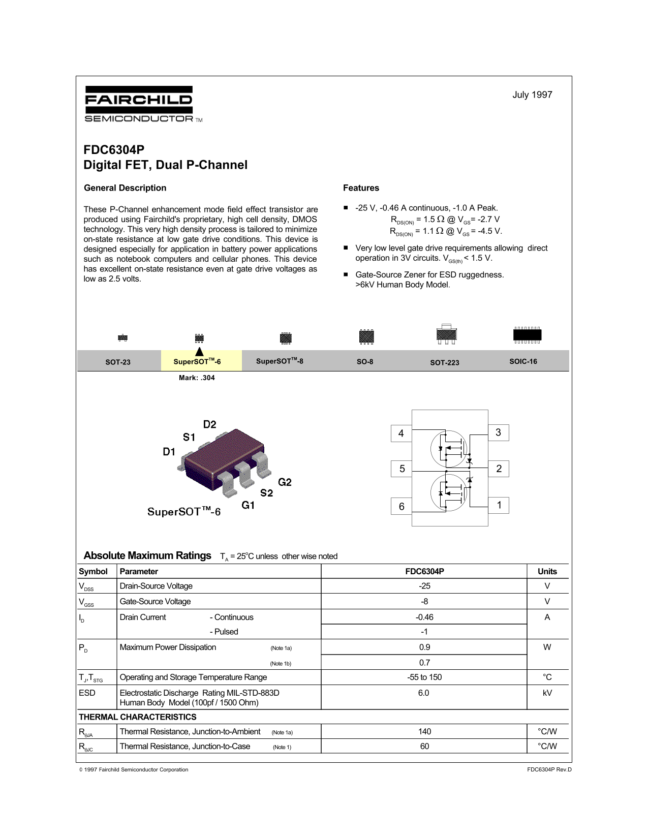
Page 1 Text Content
July 1997
FDC6304P Digital FET, Dual P-Channel General Description Features
These P-Channel enhancement mode field effect transistor are -25 V, -0.46 A continuous, -1.0 A Peak.
produced using Fairchild's proprietary, high cell density, DMOS RDS(ON) = 1.5 Ω @ VGS= -2.7 V technology. This very high density process is tailored to minimize RDS(ON) = 1.1 Ω @ VGS = -4.5 V. on-state resistance at low gate drive conditions. This device is
designed especially for application in battery power applications Very low level gate drive requirements allowing direct such as notebook computers and cellular phones. This device operation in 3V circuits. VGS(th) < 1.5 V.
has excellent on-state resistance even at gate drive voltages as
Gate-Source Zener for ESD ruggedness.
low as 2.5 volts.
>6k V Human Body Model.
SOT-23 Super SOTTM-8 SOT-223Super SOTTM-6 SOIC-16SO-8
Mark: .304
Absolute Maximum Ratings TA = 25o C unless other wise noted Symbol Parameter FDC6304P Units VDSS Drain-Source Voltage -25
VGSS Gate-Source Voltage -8
ID Drain Current - Continuous -0.46
- Pulsed -1
PD Maximum Power Dissipation (Note 1a) 0.9
(Note 1b) 0.7
TJ,TSTG Operating and Storage Temperature Range -55 to 150 °C
ESD Electrostatic Discharge Rating MIL-STD-883D 6.0 k V
Human Body Model (100pf / 1500 Ohm)
THERMAL CHARACTERISTICS
RθJA Thermal Resistance, Junction-to-Ambient (Note 1a) °C/W
RθJC Thermal Resistance, Junction-to-Case (Note 1) °C/W
© 1997 Fairchild Semiconductor Corporation FDC6304P Rev.D
Page Summary Contents For Fairchild FDC6304P User's Manual
Manual Details
| Brand | Fairchild |
|---|---|
| Pages | 5 |
| File Size | 80.43 KB |
| Published | July 06, 2026 |
Enter the captcha to get the download link:

Frequently Asked Questions
Is this FET suitable for battery-powered applications?
Yes, it has low gate drive requirements and excellent on-state resistance even at voltages as low as 2.5 volts.
What are the maximum operating temperature ranges?
The device is rated for an operating and storage temperature range of -55 to 150 °C.
Can this component be used in life support systems?
No, its use as a critical component in life support devices requires express written approval from Fairchild Semiconductor Corporation.