Fairchild FDC2512 User Guide
Summary
The FDC2512 is a high-performance N-Channel Power Trench MOSFET engineered for superior efficiency in DC/DC converters. Optimized through advanced trench technology, this component features extremely low on-resistance and fast switching speed, making it ideal for demanding power management applications. This manual provides comprehensive data, including electrical characteristics, thermal specifications, and dynamic timing parameters necessary for engineers designing reliable and high-efficiency power conversion circuitry.
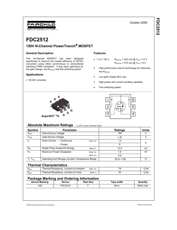
Page 1 Text Content
October 2009
FDC2512 150V N-Channel Power Trench MOSFET General Description Features This N-Channel MOSFET has been designed
• 1.4 A, 150 V. RDS(ON) = 425 mΩ @ VGS = 10 V
specifically to improve the overall efficiency of DC/DC
RDS(ON) = 475 mΩ @ VGS = 6 V
converters using either synchronous or conventional switching PWM controllers. It has been optimized for
• High performance trench technology for extremely
low gate charge, low RDS(ON) and fast switching speed.
low RDS(ON)
Applications
• Low gate charge (8n C typ)
• DC/DC converter
• High power and current handling capability
• Fast switching speed
Super SOT -6TM
Absolute Maximum Ratings TA=25o C unless otherwise noted Symbol Parameter Ratings Units VDSS Drain-Source Voltage 150 V VGSS Gate-Source Voltage ± 20 V ID Drain Current – Continuous (Note 1a) 1.4 – Pulsed 8 EAS Single Pulse Avalanche Energy 13.5 m J (Note 3)
Maximum Power Dissipation (Note 1a) 1.6 W PD (Note 1b) 0.8
TJ, Tstg Operating and Storage Junction Temperature Range −55 to +150 °C
Thermal Characteristics RθJA Thermal Resistance, Junction-to-Ambient (Note 1a) 78 °C/W RθJC Thermal Resistance, Junction-to-Case (Note 1) 30 °C/W
Package Marking and Ordering Information Device Marking Device Reel Size Tape width Quantity .252 FDC2512 7’’ 8mm 3000 units
2009 Fairchild Semiconductor Corporation FDC2512 Rev B4 (W)
Page Summary Contents For Fairchild FDC2512 User Guide
Manual Details
| Brand | Fairchild |
|---|---|
| Pages | 5 |
| File Size | 242.46 KB |
| Published | June 20, 2026 |
Enter the captcha to get the download link:

Frequently Asked Questions
What is the absolute maximum drain-source voltage ($V_{DSS}$)?
The Drain-Source Voltage has an absolute maximum rating of 150 V.
What specific types of converters is this MOSFET optimized for?
It is designed to improve efficiency in DC/DC converters using synchronous or conventional switching PWM controllers.
How much heat can it dissipate per watt (Junction-to-Ambient)?
The thermal resistance, junction-to-ambient ($ heta_{JA}$), is rated at 78 °C/W.
Where should I purchase this component to ensure it is genuine?
Buy parts directly from Fairchild or via an Authorized Fairchild Distributor listed by country on their website.