Fairchild Fan5362 User's Manual
Summary
The FAN5362 is a high-efficiency 3MHz synchronous buck regulator offering 500mA or 750mA output current. Ideal for smartphones and portable devices, it features a fixed 1.8V to 3.6V output, wide input range, and PFM mode for superior light-load efficiency.
Page 1 Text Content
5362 — 3M z, 500m / 750m yn ch ro s B ck R eg lato
September 2011
FAN5362 3MHz, 500m A / 750m A Synchronous Buck Regulator Features Description
3MHz Fixed-Frequency Operation The FAN5362 is a 500m A or 750m A, step-down, switching voltage regulator that delivers a fixed output voltage from
45µA Typical Quiescent Current
an input voltage supply of 2.7V to 5.5V. Using a proprietary 1.80 to 3.6V Fixed Output Voltage architecture with synchronous rectification, the FAN5362 is capable of delivering a peak efficiency of 96%, while
500m A or 750m A Output Current Capability
maintaining efficiency over 90% with load currents as
2.7V to 5.5V Input Voltage Range low as 1m A. Smooth Transitions to/from 100% Duty Cycle
This regulator transitions seamlessly into and out of 100%
when VIN Drops
duty cycle operation when the supply dips to or below the PFM Mode for High Efficiency in Light Load regulation setpoint and smoothly recovers full regulation without overshoot when the supply recovers.
Best-in-Class Load Transient Response
The regulator operates at a nominal fixed frequency of
Best-in-Class Efficiency
3MHz, which reduces the value of the external components
Forced PWM and External Clock Synchronization to 1µH for the output inductor and 4.7µF for the output
Internal Soft-Start capacitor. The PWM modulator can be synchronized to an external frequency source.
Input Under-Voltage Lockout (UVLO)
At moderate and light loads, pulse frequency modulation is
Thermal Shutdown and Overload Protection
used to operate the device in power-save mode with a
6-Bump WLCSP, 0.4mm Pitch or 6-Lead 2 x 2mm typical quiescent current of 45µA. Even with such a low Ultrathin Molded Leadless Package quiescent current, the part exhibits excellent transient
response during large load swings. At higher loads, the system automatically switches to fixed-frequency control,
Applications
operating at 3MHz. In shutdown mode, the supply current drops below 1µA, reducing power consumption. For
SD Flash Memory Power Supply
applications that require minimum ripple or fixed frequency,
RF Transceiver Power PFM mode can be disabled using the MODE pin. Cell Phones, Smart Phones
The FAN5362 is available in 6-bump, 0.4mm pitch, Wafer- Tablets, Netbooks®, Ultra-Mobile PCs Level Chip-Scale Package (WLCSP) and 6-Lead 2 x 2mm Ultrathin Molded Leadless Package (UMLP).
3G, LTE, Wi MAX™, Wi Bro®, and Wi Fi® Data Cards Gaming Devices, Digital Cameras DC/DC Micro Modules
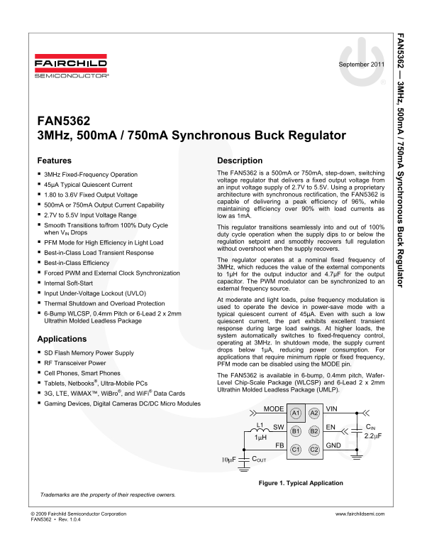
MODE VIN
SW ENL1 CIN
FB GND C1 C2
Figure 1. Typical Application
Trademarks are the property of their respective owners.
© 2009 Fairchild Semiconductor Corporation www.fairchildsemi.com FAN5362 • Rev. 1.0.4
Page Summary Contents For Fairchild Fan5362 User's Manual
Manual Details
| Brand | Fairchild |
|---|---|
| Pages | 14 |
| File Size | 1.18 MB |
| Published | June 15, 2026 |
Enter the captcha to get the download link:

Frequently Asked Questions
What is the input voltage range of the FAN5362?
2.7V to 5.5V.
How do I enable or disable the device?
Enable pin: >1.2V enables, <0.4V shuts down; do not float.
What is the typical quiescent current?
45µA typical in power-save mode (PFM).
Can the switching frequency be synchronized externally?
Yes, through the MODE pin, synchronizes to two times the external frequency.