# A B C D E F G H I J K L M N O P Q R S T U V W X Y Z

FAIRCHILD FAN5361 User Guide

Summary

The FAN5361 is a high-performance, miniature synchronous buck regulator designed for mobile and low-power electronics requiring reliable fixed-frequency power conversion. It delivers up to 750mA output current with best-in-class efficiency (up to 92%) while maintaining an extremely low quiescent current of 35µA. This manual provides complete technical specifications, including operating modes, voltage ranges, and protection features necessary for integrating this regulator into devices such as smartphones, tablets, netbooks, data cards, and ultra-mobile PCs needing stable, ripple-free power.
📄 Preview PAGE OF 18

Page 1 Text Content

5361 — 6M z, 600m / 750m yn ch ro s B ck R eg lato

June 2011

FAN5361 6MHz, 600m A / 750m A Synchronous Buck Regulator

Features Description  6MHz Fixed-Frequency Operation The FAN5361 is a 600m A or 750m A, step-down, switching voltage regulator that delivers a fixed output from a 2.3V to

 35µA Typical Quiescent Current

5.5V input voltage supply. Using a proprietary architecture

 Best-in-Class Load Transient Response

with synchronous rectification, the FAN5361 is capable of

 Best-in-Class Efficiency

delivering a peak efficiency of 92%, while maintaining

 600m A or 750m A Output Current Capability efficiency over 80% at load currents as low as 1m A.  2.3V to 5.5V Input Voltage Range

The regulator operates at a nominal fixed frequency of

 1.0 to 1.90V Fixed Output Voltage

6MHz, which reduces the value of the external components

 Low Ripple Light-Load PFM Mode to 470n H for the output inductor and 4.7µF for the output

 Forced PWM and External Clock Synchronization capacitor. The PWM modulator can be synchronized to an external frequency source.

 Internal Soft-Start  Input Under-Voltage Lockout (UVLO) At moderate and light loads, pulse frequency modulation is

 Thermal Shutdown and Overload Protection used to operate the device in power-save mode with a typical quiescent current of 35µA. Even with such a low

 6-bump WLCSP, 0.4mm Pitch

quiescent current, the part exhibits excellent transient

 6-pin 2 x 2mm UMLP

response during large load swings. At higher loads, the system automatically switches to fixed-frequency control,

Applications

operating at 6MHz. In shutdown mode, the supply current  Cell Phones, Smart Phones drops below 1µA, reducing power consumption. For applications that require minimum ripple or fixed frequency,

 Tablets, Netbooks®, Ultra-Mobile PCs

PFM mode can be disabled using the MODE pin.

 3G, LTE, Wi MAX™, Wi Bro®, and Wi Fi® Data Cards

 Gaming Devices, Digital Cameras DC/DC Micro Modules The FAN5361 is available in 6-bump, 0.4mm pitch, Wafer- Level Chip-Scale Package (WLCSP) and a 6-lead 2 x 2mm ultra-thin MLP package (UMLP).

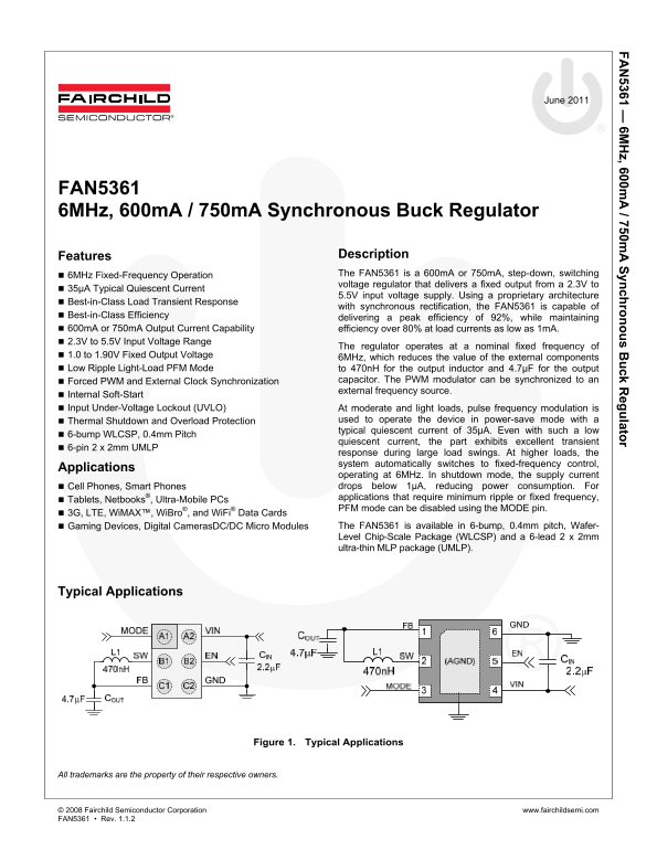
Typical Applications

Figure 1. Typical Applications

All trademarks are the property of their respective owners.

© 2008 Fairchild Semiconductor Corporation www.fairchildsemi.com FAN5361 • Rev. 1.1.2

Page Summary Contents For FAIRCHILD FAN5361 User Guide

Page 1 5361 — 6M z, 600m / 750m yn ch ro s B ck R eg lato June 2011 FAN5361 6MHz, 600m A / 750m A Synchronous Buck Regulator Features Description  6MHz Fixed-Frequency Operation The FAN5361 is a 600m A or 7...
Page 2 5361 — 6M z, 600m / 750m yn ch ro s B ck R eg lato Ordering Information Output Part Number Package Temperature Range Packing Voltage(1) FAN5361UC123X 1.233V FAN5361UC182X 1.820V WLCSP-6, 0.4mm Pitch F...
Page 3 5361 — 6M z, 600m / 750m yn ch ro s B ck R eg lato Absolute Maximum Ratings Stresses exceeding the absolute maximum ratings may damage the device. The device may not function or be operable above the ...
Page 4 5361 — 6M z, 600m / 750m yn ch ro s B ck R eg lato Electrical Characteristics Minimum and maximum values are at VIN = VEN = 2.3V to 5.5V, VMODE = 0V (AUTO Mode), TA = -40°C to +85°C; circuit of Figure...
Page 5 5361 — 6M z, 600m / 750m yn ch ro s B ck R eg lato (V ff ic ie ff ic ie cy Typical Performance Characteristics Unless otherwise noted, VIN = VEN = 3.6V, VMODE = 0V (AUTO Mode), VOUT = 1.82V, TA = 25°C...
Page 6 5361 — 6M z, 600m / 750m yn ch ro s B ck R eg lato it ch in re en cy z) (V Typical Performance Characteristics (Continued) Unless otherwise noted, VIN = VEN = 3.6V, VMODE = 0V (AUTO Mode), VOUT = 1.82...
Page 7 5361 — 6M z, 600m / 750m yn ch ro s B ck R eg lato rr (m Typical Performance Characteristics (Continued) Unless otherwise noted, VIN = VEN = 3.6V, VMODE = 0V (AUTO Mode), VOUT = 1.82V, TA = 25°C. Alwa...
Page 8 5361 — 6M z, 600m / 750m yn ch ro s B ck R eg lato Typical Performance Characteristics (Continued) Unless otherwise noted, VIN = VEN = 3.6V, VMODE = 0V (AUTO Mode), VOUT = 1.82V, TA = 25°C, 5µs/div. h...
Page 9 5361 — 6M z, 600m / 750m yn ch ro s B ck R eg lato Typical Performance Characteristics (Continued) Unless otherwise noted, VIN = VEN = 3.6V, VMODE = 0V (AUTO Mode), VOUT = 1.82V, TA = 25°C, 5µs/div. h...
Page 10 5361 — 6M z, 600m / 750m yn ch ro s B ck R eg lato Typical Performance Characteristics (Continued) Unless otherwise noted, VIN = VEN = 3.6V, VMODE = 0V (AUTO Mode), VOUT = 1.82V, TA = 25°C, 5µs/div. h...
Page 11 5361 — 6M z, 600m / 750m yn ch ro s B ck R eg lato Typical Performance Characteristics (Continued) Unless otherwise noted, VIN = VEN = 3.6V, VMODE = 0V (AUTO Mode), VOUT = 1.82V, TA = 25°C. Figure 39....
Page 12 5361 — 6M z, 600m / 750m yn ch ro s B ck R eg lato Operation Description The FAN5361 is a 600m A or 750m A, step-down, switching To prevent shut-down during soft-start, the following condition voltage...
Page 13 5361 — 6M z, 600m / 750m yn ch ro s B ck R eg lato Under-Voltage Lockout (UVLO) When VIN is LOW, fixed switching is maintained as long as When EN is HIGH, the under-voltage lockout keeps the part OUT ...
Page 14 5361 — 6M z, 600m / 750m yn ch ro s B ck R eg lato Applications Information Selecting the Inductor I I  (8) The output inductor must meet both the required inductance )DC(OUTRMS and the energy handl...
Page 15 5361 — 6M z, 600m / 750m yn ch ro s B ck R eg lato PCB Layout Guidelines There are only three external components: the inductor and erratically due to excessive noise. This reduces switching the input...
Page 16 5361 — 6M z, 600m / 750m yn ch ro s B ck R eg lato Physical Dimensions BALL A1 INDEX AREA Cu Pad (Ø0.30) Solder Mask Opening TOP VIEW RECOMMENDED LAND PATTERN (NSMD PAD TYPE) SEATING PLANE SIDE VIEWS ...
Page 17 5361 — 6M z, 600m / 750m yn ch ro s B ck R eg lato Physical Dimensions PIN1 IDENT TOP VIEW 0.55 MAX 0.65 0.10 RECOMMENDED LAND PATTERN SEATING PLANE SIDE VIEW NOTES: 1.50 A. OUTLINE BASED ON JEDEC REG...
Page 18 5361 — 6M z, 600m / 750m yn ch ro s B ck R eg lato © 2008 Fairchild Semiconductor Corporation www.fairchildsemi.com FAN5361 • Rev. 1.1.2 18

Manual Details

Brand Fairchild
Pages 18
File Size 926.22 KB
Published June 20, 2026
2 views

Enter the captcha to get the download link:

captcha

Frequently Asked Questions

What input voltage range does the FAN5361 support?

The regulator operates within an input voltage range of 2.3V to 5.5V.

How can I force the device into PWM mode instead of PFM?

Apply a logic 1 signal to the MODE pin to keep the IC in forced PWM mode.

What are the maximum continuous current outputs for this regulator?

It supports 600mA or 750mA output currents.

Which types of devices can use the FAN5361 regulator as an application example?

Recommended applications include Cell Phones, tablets, netbooks, and data cards.