Fairchild BSP52 NPN Darlington Transistor User's Guide
Summary
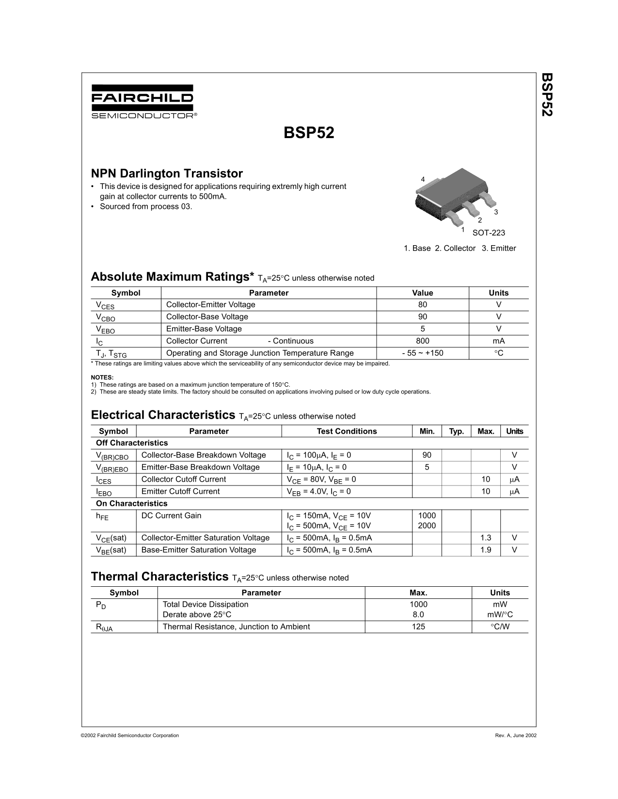
This datasheet describes the Fairchild BSP52 NPN Darlington transistor in SOT-223 surface-mount package, designed for applications requiring extremely high current gain at collector currents up to 500mA. The device is rated for 80V collector-emitter voltage, 90V collector-base voltage, and 800mA continuous collector current with 150°C maximum junction temperature. DC current gain (hFE) reaches 1000 minimum at 150mA/10V and 2000 minimum at 500mA/10V, with collector-emitter saturation voltage of 1
Page 1 Text Content
BSP52
NPN Darlington Transistor This device is designed for applications requiring extremly high current gain at collector currents to 500m A. Sourced from process 03.
SOT-2231
1. Base 2. Collector 3. Emitter
Absolute Maximum Ratings* TA=25°C unless otherwise noted Symbol Parameter Value Units VCES Collector-Emitter Voltage
VCBO Collector-Base Voltage
VEBO Emitter-Base Voltage
IC Collector Current - Continuous m A TJ, TSTG Operating and Storage Junction Temperature Range - 55 ~ +150 °C
* These ratings are limiting values above which the serviceability of any semiconductor device may be impaired.
NOTES: 1) These ratings are based on a maximum junction temperature of 150°C. 2) These are steady state limits. The factory should be consulted on applications involving pulsed or low duty cycle operations.
Electrical Characteristics TA=25°C unless otherwise noted Symbol Parameter Test Conditions Min. Typ. Max. Units Off Characteristics
V(BR)CBO Collector-Base Breakdown Voltage IC = 100µA, IE = 0 V(BR)EBO Emitter-Base Breakdown Voltage IE = 10µA, IC = 0 ICES Collector Cutoff Current VCE = 80V, VBE = 0 µA IEBO Emitter Cutoff Current VEB = 4.0V, IC = 0 µA
On Characteristics h FE DC Current Gain IC = 150m A, VCE = 10V
IC = 500m A, VCE = 10V
VCE(sat) Collector-Emitter Saturation Voltage IC = 500m A, IB = 0.5m A 1.3 VBE(sat) Base-Emitter Saturation Voltage IC = 500m A, IB = 0.5m A 1.9
Thermal Characteristics TA=25°C unless otherwise noted Symbol Parameter Max. Units PD Total Device Dissipation m W
Derate above 25°C 8.0 m W/°C RθJA Thermal Resistance, Junction to Ambient °C/W
©2002 Fairchild Semiconductor Corporation Rev. A, June 2002
Page Summary Contents For Fairchild BSP52 NPN Darlington Transistor User's Guide
Manual Details
| Brand | Fairchild |
|---|---|
| Pages | 3 |
| File Size | 37.25 KB |
| Published | July 06, 2026 |
Enter the captcha to get the download link:

Frequently Asked Questions
What is the maximum continuous collector current rating for this device?
The specified collector current ($I_C$) is -800 mA.
How should I derate dissipation if operating above 25°C?
You must apply a derating rate of 8.0 mW/°C.
Can this transistor be used in life support devices or systems?
No, it is not authorized for use as critical components in life support devices without express written approval.
What are the typical DC current gains at specified test conditions?
The typical $h_{FE}$ and $h_{FC}$ gains are 1000 and 2000, respectively.