Page 1
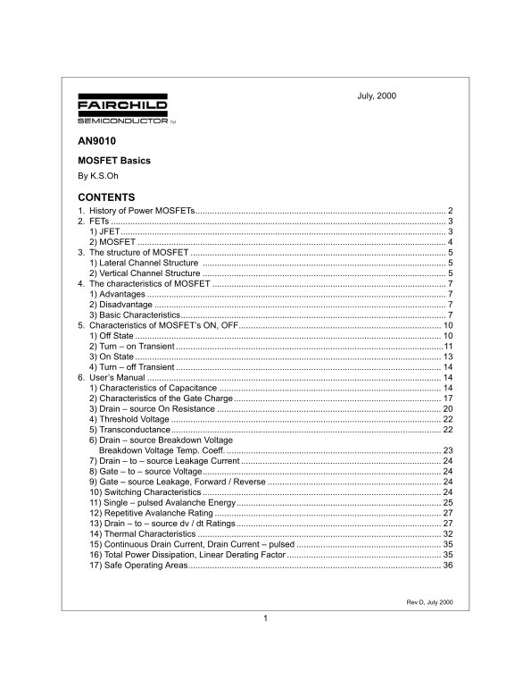
July, 2000 AN9010 MOSFET Basics By K.S.Oh CONTENTS 1. History of Power MOSFETs........................................................................................................ 2. FETs 1) JFET.....
Page 2
The Bipolar Power Transistor (BPT), as a switching device for power applications, had a few disad- vantages. This led to the development of the power MOSFET (Metal Oxide Semiconductor Field Effect Tra...
Page 3
2. FETs JFET, MOSFET 1) JFET (Junction Field Effect Transistors) There are two types of JFETs. One is an n-channel type and the other is a p-channel type. They both control the drain-to-source current...
Page 4
2) MOSFET (Metal Oxide Semiconductor Field Effect Transistors) The two types of MOSFETs are the depletion type and the enhancement type, and each has a n / p – channel type. The depletion type is norm...
Page 5
3. The Structure of a MOSFET 1) Lateral Channel Design The drain, gate, and source terminal are placed on the surface of a silicon wafer. This is suitable for integration but not for obtaining high po...
Page 6
Source Source P-body P-body P-body P-body N— epitaxial layer N— epitaxial layer N+ substrate N+ substrate Drain Drain Source P-body P-body N— epitaxial layer N+ substrate Drain Figure 4: Vertical Chan...
Page 7
4. The Characteristics of a MOSFET 1) Advantages 1. High input impedance - voltage controlled device - easy to drive. To maintain the on-state, a base drive current which is 1/5th or 1/10th of collect...
Page 8
But if the VDS rate of increase is large in the high speed turn–off state, there is a voltage drop between the base and the emitter, which causes the BJT to turn–on. This is prevented by increasing th...
Page 9
[VGS — VGS(th) = VDS] i D Ohmic Active VGS5 > VGS4 > VGS3 > VGS2 > VGS1 Cutoff VGS < VGS(th) VGS2 VGS1 BVDSS Figure 6: Output Characteristics 4. Transfer characteristics i D characteris...
Page 10
increase of the electric field along with the increase of i D at the inverse layer. Actual Linearized VGS(th) Figure 7: Transfer Curve 5. Characteristics of MOSFET’s in ON and OFF States. 1) Off State...
Page 11
2) Turn-on Transient The Process of Channel Formation 1. The formation of the depletion region: When a small positive gate – to – source voltage is supplied to the gate electrode (refer to Fig- ure 8 ...
Page 12
VGG1 VGG2 Ionized acceptors Free electrons Depletion region boundary Inversion VGG3 > V GG2 > V GG1 Figure 8: The Process of Channel Formation (a) Formation of the Depletion Region (b), (c) Form...
Page 13
3) On state Drain current (ID) changes due to the increase in drain-to-source voltage (VDD) (VGS is constant). ID starts to flow when the channel has formed and VDD is supplied. When the VGS is a cons...
Page 14
The velocity of the charge carrier increases with the increase in the electric field initially, and at a certain point, it is saturated. Silicon starts saturating when the electric field reaches 1.5x1...
Page 15
(1): CGS: The Capacitance between the Gate and Source Cgs CO CP+ 1. CO: The capacitance between the gate and source metal εIAO CO t O where εI: the dielectric constant of the intervening insulator t O...
Page 16
Wd(epi.): the width of the depletion region in the epitaxial layer(= N- drift region) 2ksεo VDS φB+( Wd(epi.) As Cgd increases (1+gfs RL(load resistance)) times due to the Miller effect, it prominentl...
Page 17
2) Characteristics of the Gate Charge It is the amount of charge that is required during the MOSFET’s turn-on or turn-off transient. The following types of charges are mentioned In the data book. Tota...
Page 18
VDD VDD IODF IODF Cgd1 Cd Cgd1 Cd RG RG VGG i G VGG i G Cgs Cgs VDD VDD IO IO VGG r DS(on) VGG i G Figure 13: Equivalent Circuits of the MOSFET with Turn-on Divided into 4 Periods at the Diode-clamped...
Page 19
The following graph shows the VGS(t) measuring the Va variation in accordance with i D condi- tions in turn-on state. VGS(t) IO = 10[A] IO = 7[A] IO = 3[A] Device: FQP10N20 Test Condition: VDS = 160[V...
Page 20
The following figure graphs VGS(t) and shows the variation of t2 ~ t3 (flat region of VGS) in accordance with the VDD condition. VGS(t) VDD = 160[V] VDD = 100[V] VDD = 40[V] Device: FQP10N20 Test Cond...
Page 21
In a MOSFET RDS(on) is the total resistance between the source and the drain during the on state, and it is an important parameter determining maximum current rating and loss. To reduce RDS(on), the i...
Page 22
4) Threshold Voltage (VGS(th)) This is the minimum gate bias which enables the formation of the channel between the source and 2 in the saturation region. the drain. The drain current increases in pro...
Page 23
Actual GS Linearized GSv )th(GSV Figure 15: Transfer Curve & gfs Temperature characteristic gfs decreases as the temperature increases due to the reduction of mobility. From the following equation...
Page 24
Temperature characteristic As junction temperature increases, it does so linearly, and whenever it goes up 100 [°C], 10[%] of BVDSS at 25 [°C] increases (refer to the breakdown voltage temperature coe...
Page 25
td(on)(turn-on delay time): This is the time for the gate voltage VGS to reach up to the threshold voltage VGS(th). The input capacitance during this period is Cgs+Cgd. This also means that this perio...
Page 26
reduce, the inductive load increases the drain voltage so that it maintains the drain current. When the drain voltage increases, the drain current is divided into the channel current and the displace-...
Page 27
(2) A power MOSFET Failure has the following characteristics during an inductive turn-off. 1. It has the same electrical characteristics as the second breakdown of the bipolar transistor. 2. Independe...
Page 28
Drain dv dt Source Figure 18: Equivalent Circuit of a N-channel MOSFET 1. In the off state, a sudden increase in drain voltage changes the voltage across the parasitic capacitance between the drain an...
Page 29
transistor is turned on, the breakdown voltage of the device is reduced from BVCBO to BVCEO which is 50 ~ 60 [%] of BVCBO. If a drain voltage larger than BVCEO is supplied, the device falls into an av...
Page 30
(3) Diode Recovery dv/dt This is the main cause of dv/dt failure in specific applications such as circuits using a body drain diode. The data book gives the maximum value for dv/dt. Exceeding this val...
Page 31
Driver RG Same Type as DUT *dv/dt controlled by RG *IS controlled by pulse period GSV Width Pulse Gate (Driver) Period Pulse Gate IFM, Body Diode Forward Current di/dt (DUT) rrt Body Diode Reverse Cur...
Page 32
The value of di/dt and dv/dt becomes larger as RG is reduced. First trr can be obtained by measur- ing the part shown in the wave of IS where the di/dt (It is measured from the point where it is 50[%]...
Page 33
Junction Case Sink Ambient RθJC RθCS RθSA TJ TC TS TA Figure 22: An Equivalent Circuit Based on Thermal Resistance As shown in Figure 21, the heat produced at the chip junction normally discharges ove...
Page 34
Thermal Response Characteristics In Figure 11 in the data book, the graph of the thermal response shows the change of ZθJC(t) (junc- tion– to–case thermal impedance) due to the change of the square wa...
Page 35
15) Continuous Drain Current (ID), Drain Current - Pulsed (IDM) (1) Continuous Drain Current (ID) As shown in the equation below, the ID rating is determined by the heat removal ability of the device....
Page 36
17) Safe Operating Areas (SOA) (1) SOA (FBSOA): It defines the maximum value of the drain – source voltage and drain current which guarantees safe operation when the device is at the forward bias. (2)...
Page 37
TRADEMARKS The following are registered and unregistered trademarks Fairchild Semiconductor owns or is authorized to use and is not intended to be an exhaustive list of all such trademarks. ACEx™ Hi S...