ANALOG DEVICES AD5160 256-Position SPI Compatible Digital Potentiometer
Summary
The AD5160 is a compact digital potentiometer providing 256 positions of precise variable resistance control in an SOT-23-8 package. It functions as a solid-state replacement for bulky mechanical potentiometers, offering superior reliability and low temperature coefficient performance. Controllable via an SPI interface and operating within a wide temperature range, this module is ideal for electronics designers requiring highly accurate adjustment in applications such as sensor biasing (pressure/temp), automotive systems, and RF amplifier design.
Page 1 Text Content
256-Position SPI Compatible Digital Potentiometer
AD5160
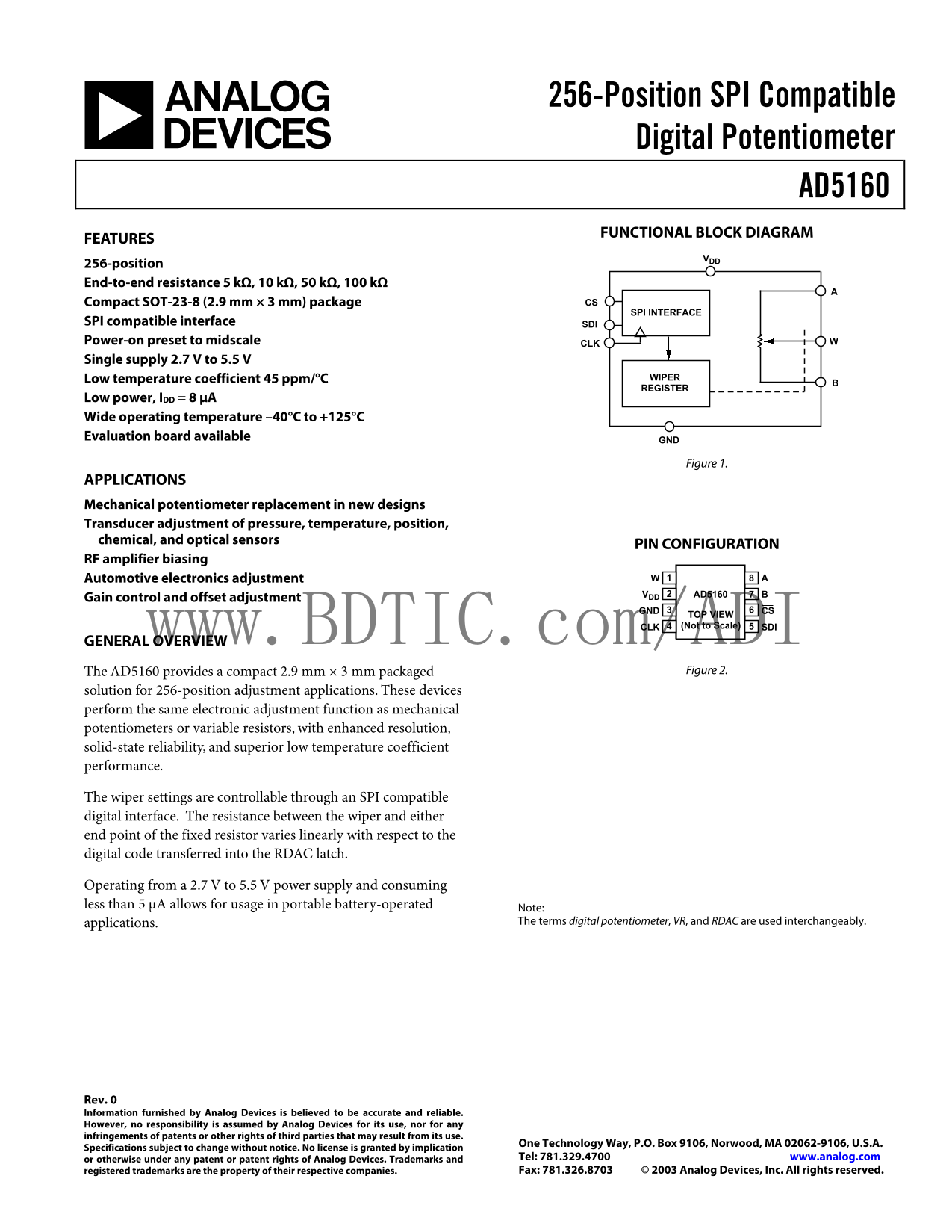
FUNCTIONAL BLOCK DIAGRAM
FEATURES
256-position End-to-end resistance 5 kΩ, 10 kΩ, 50 kΩ, 100 kΩ
Compact SOT-23-8 (2.9 mm × 3 mm) package CS
SPI INTERFACE
SPI compatible interface SDI Power-on preset to midscale CLK Single supply 2.7 V to 5.5 V
Low temperature coefficient 45 ppm/°C WIPER REGISTER
Low power, IDD = 8 µA Wide operating temperature –40°C to +125°C Evaluation board available GND
Figure 1.
APPLICATIONS Mechanical potentiometer replacement in new designs Transducer adjustment of pressure, temperature, position, chemical, and optical sensors
PIN CONFIGURATION
RF amplifier biasing Automotive electronics adjustment
VDD AD5160
Gain control and offset adjustment
GND CS
TOP VIEW CLK (Not to Scale) SDI
GENERAL OVERVIEW www.BDTIC.com/ADI
The AD5160 provides a compact 2.9 mm × 3 mm packaged Figure 2.
solution for 256-position adjustment applications. These devices perform the same electronic adjustment function as mechanical potentiometers or variable resistors, with enhanced resolution, solid-state reliability, and superior low temperature coefficient performance.
The wiper settings are controllable through an SPI compatible digital interface. The resistance between the wiper and either end point of the fixed resistor varies linearly with respect to the digital code transferred into the RDAC latch.
Operating from a 2.7 V to 5.5 V power supply and consuming less than 5 µA allows for usage in portable battery-operated Note:
applications. The terms digital potentiometer, VR, and RDAC are used interchangeably.
Rev. 0 Information furnished by Analog Devices is believed to be accurate and reliable. However, no responsibility is assumed by Analog Devices for its use, nor for any infringements of patents or other rights of third parties that may result from its use.
One Technology Way, P.O. Box 9106, Norwood, MA 02062-9106, U.S.A.
Specifications subject to change without notice. No license is granted by implication
or otherwise under any patent or patent rights of Analog Devices. Trademarks and Tel: 781.329.4700 www.analog.com registered trademarks are the property of their respective companies. Fax: 781.326.8703 © 2003 Analog Devices, Inc. All rights reserved.
Page Summary Contents For ANALOG DEVICES AD5160 256-Position SPI Compatible Digital Potentiometer
Manual Details
| Brand | Analog Devices |
|---|---|
| Pages | 16 |
| File Size | 723.48 KB |
| Published | July 16, 2026 |
Enter the captcha to get the download link:

Frequently Asked Questions
What is the operating voltage range for the AD5160?
It operates from a single supply of 2.7 V to 5.5 V.
How does the user control the resistance adjustment?
The wiper settings are controlled through an SPI compatible digital interface.
What is the low-temperature coefficient performance at the AD5160?
It features a superior low temperature coefficient of 45 ppm/°C.
What power consumption can I expect from this device?
It consumes very little power, less than 5 µA.
Are there different resistance options available?
Yes, available end-to-end resistances include 5 kΩ, 10 kΩ, 50 kΩ, and 100 kΩ.