ANALOG DEVICES AD620 User Guide
Summary
The AD620 is a premium, low-cost instrumentation amplifier designed for demanding applications requiring high precision and minimal power consumption. This technical resource provides comprehensive details on the amplifier’s performance, including circuit diagrams, ideal operating ranges (1 to 10,000 gain), and advanced specifications such as ultra-low noise and offset drift. It is essential reading for engineers developing sensitive equipment like ECG monitors, weigh scales, industrial process controls, or any battery-powered data acquisition system where accuracy is critical.
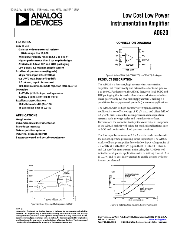
Page 1 Text Content
Low Cost Low Power Instrumentation Amplifier
TO TA ER , P PM FU LL LE
AD620 FEATURES
CONNECTION DIAGRAM
Easy to use Gain set with one external resistor
RG RG
(Gain range 1 to 10,000)
–IN +VS
Wide power supply range (±2.3 V to ±18 V)
Higher performance than 3 op amp IA designs +IN OUTPUT
Available in 8-lead DIP and SOIC packaging –VS 5AD620 REF
Low power, 1.3 m A max supply current
TOP VIEW
Excellent dc performance (B grade) 50 µV max, input offset voltage 5- 0- Figure 1. 8-Lead PDIP (N), CERDIP (Q), and SOIC (R) Packages
0.6 µV/°C max, input offset drift
PRODUCT DESCRIPTION
1.0 n A max, input bias current
The AD620 is a low cost, high accuracy instrumentation
100 d B min common-mode rejection ratio (G = 10)
amplifier that requires only one external resistor to set gains of
Low noise
1 to 10,000. Furthermore, the AD620 features 8-lead SOIC and
9 n V/√Hz @ 1 k Hz, input voltage noise
DIP packaging that is smaller than discrete designs and offers
0.28 µV p-p noise (0.1 Hz to 10 Hz)
lower power (only 1.3 m A max supply current), making it a
Excellent ac specifications
good fit for battery-powered, portable (or remote) applications.
120 k Hz bandwidth (G = 100) 15 µs settling time to 0.01% The AD620, with its high accuracy of 40 ppm maximum
TI LT IS (0 .1 z) p- p) nonlinearity, low offset voltage of 50 µV max, and offset drift of
APPLICATIONS 0.6 µV/°C max, is ideal for use in precision data acquisition systems, such as weigh scales and transducer interfaces.
Weigh scales
Furthermore, the low noise, low input bias current, and low power
ECG and medical instrumentation
of the AD620 make it well suited for medical applications, such
Transducer interface
as ECG and noninvasive blood pressure monitors.
Data acquisition systems Industrial process controls
The low input bias current of 1.0 n A max is made possible with
Battery-powered and portable equipment
the use of Superϐeta processing in the input stage. The AD620 works well as a preamplifier due to its low input voltage noise of 9 n V/√Hz at 1 k Hz, 0.28 µV p-p in the 0.1 Hz to 10 Hz band, and 0.1 p A/√Hz input current noise. Also, the AD620 is well
suited for multiplexed applications with its settling time of 15 µs to 0.01%, and its cost is low enough to enable designs with one
in-amp per channel.
25,000 3 OP AMP
IN-AMP 1,000
(3 OP-07s) TYPICAL STANDARD
20,000 BIPOLAR INPUT IN-AMP
AD620A
AD620 SUPERβETA BIPOLAR INPUT IN-AMP
SUPPLY CURRENT (m A) SOURCE RESISTANCE (Ω)
Figure 2. Three Op Amp IA Designs vs. AD620
Figure 3. Total Voltage Noise vs. Source Resistance
Rev. G Information furnished by Analog Devices is believed to be accurate and reliable. However, no responsibility is assumed by Analog Devices for its use, nor for any infringements of patents or other rights of third parties that may result from its use.
One Technology Way, P.O. Box 9106, Norwood, MA 02062-9106, U.S.A.
Specifications subject to change without notice. No license is granted by implication
or otherwise under any patent or patent rights of Analog Devices. Trademarks and Tel: 781.329.4700 www.analog.com registered trademarks are the property of their respective owners. Fax: 781.326.8703 © 2004 Analog Devices, Inc. All rights reserved.
Page Summary Contents For ANALOG DEVICES AD620 User Guide
Manual Details
| Brand | Analog Devices |
|---|---|
| Pages | 20 |
| File Size | 561.22 KB |
| Published | May 14, 2026 |
Enter the captcha to get the download link:

Frequently Asked Questions
How do I set the gain for the AD620 amplifier?
You only require one external resistor to set gains in a wide range from 1 to 10,000.
Is this amplifier suitable for portable or battery-powered equipment?
Yes, it is excellent for remote applications due to its low power consumption and max supply current of only 1.3 mA.
What types of physical packaging are available?
The device is available in 8-lead DIP, SOIC (R), and CERDIP (Q) packages.
What key specification makes it good for medical instrumentation like ECG?
It features low noise, low input bias current, and a high common-mode rejection ratio of 100 dB min.