# A B C D E F G H I J K L M N O P Q R S T U V W X Y Z

AD5666 Analog Devices Data Sheet

Summary

This professional guide details the AD5666, a robust, low-power quad 16-bit buffered voltage DAC designed for precision control. It provides in-depth information on operating features, including simultaneous outputs, integrated high-accuracy reference voltages (1.25V or 2.5V), and rail-to-rail bandwidth. Ideal for engineers developing data acquisition systems, process controllers, and portable instruments, the manual covers setup from reset functions to serial interfacing standards like SPI/QSPI, ensuring developers can achieve maximum reliability and efficiency in demanding applications.
📄 Preview 📖 Table of Contents Contents PAGE OF 28

Page 1 Text Content

Quad, 16-Bit DAC with 5 ppm/°C On-Chip Reference in 14-Lead TSSOP

AD5666 FEATURES FUNCTIONAL BLOCK DIAGRAM

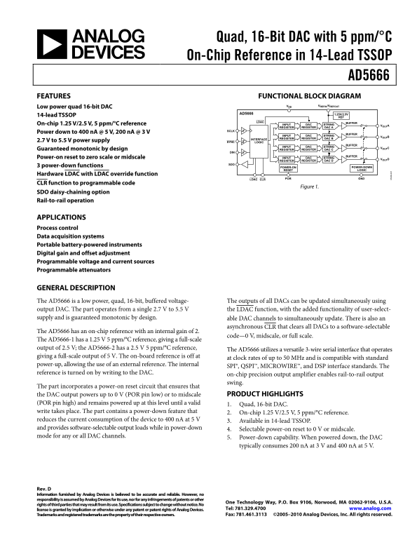
VDD VREFIN/VREFOUT

Low power quad 16-bit DAC

AD5666 1.25V/2.5V

14-lead TSSOP REF

LDAC BUFFER

On-chip 1.25 V/2.5 V, 5 ppm/°C reference INPUT DAC STRING VOUTA

REGISTER REGISTER DAC

Power down to 400 n A @ 5 V, 200 n A @ 3 V

BUFFER

INPUT DAC STRING VOUTB INTERFACE REGISTER REGISTER DAC

2.7 V to 5.5 V power supply SYNC LOGIC

BUFFER

INPUT DAC STRING VOUTC Guaranteed monotonic by design REGISTER REGISTER DAC

BUFFER

Power-on reset to zero scale or midscale INPUT DAC STRING VOUTD REGISTER REGISTER DAC

3 power-down functions POWER-ON POWER-DOWN

RESET LOGIC

Hardware LDAC with LDAC override function

LDAC CLR POR GND

CLR function to programmable code

Figure 1.

SDO daisy-chaining option Rail-to-rail operation

APPLICATIONS Process control Data acquisition systems Portable battery-powered instruments Digital gain and offset adjustment Programmable voltage and current sources Programmable attenuators

GENERAL DESCRIPTION

The AD5666 is a low power, quad, 16-bit, buffered voltage- The outputs of all DACs can be updated simultaneously using output DAC. The part operates from a single 2.7 V to 5.5 V the LDAC function, with the added functionality of user-select-

supply and is guaranteed monotonic by design. able DAC channels to simultaneously update. There is also an

asynchronous CLR that clears all DACs to a software-selectable

The AD5666 has an on-chip reference with an internal gain of 2.

code—0 V, midscale, or full scale.

The AD5666-1 has a 1.25 V 5 ppm/°C reference, giving a full-scale output of 2.5 V; the AD5666-2 has a 2.5 V 5 ppm/°C reference,

The AD5666 utilizes a versatile 3-wire serial interface that operates

giving a full-scale output of 5 V. The on-board reference is off at

at clock rates of up to 50 MHz and is compatible with standard

power-up, allowing the use of an external reference. The internal

SPI®, QSPI™, MICROWIRE™, and DSP interface standards. The

reference is turned on by writing to the DAC.

on-chip precision output amplifier enables rail-to-rail output swing.

The part incorporates a power-on reset circuit that ensures that

the DAC output powers up to 0 V (POR pin low) or to midscale PRODUCT HIGHLIGHTS

(POR pin high) and remains powered up at this level until a valid 1. Quad, 16-bit DAC. write takes place. The part contains a power-down feature that 2. On-chip 1.25 V/2.5 V, 5 ppm/°C reference. reduces the current consumption of the device to 400 n A at 5 V 3. Available in 14-lead TSSOP. and provides software-selectable output loads while in power-down 4. Selectable power-on reset to 0 V or midscale. mode for any or all DAC channels. 5. Power-down capability. When powered down, the DAC

typically consumes 200 n A at 3 V and 400 n A at 5 V.

Rev. D Information furnished by Analog Devices is believed to be accurate and reliable. However, no responsibility is assumed by Analog Devices for its use, nor for any infringements of patents or other

One Technology Way, P.O. Box 9106, Norwood, MA 02062-9106, U.S.A.

rights of third parties that may result from its use. Specifications subject to change without notice. No

license is granted by implication or otherwise under any patent or patent rights of Analog Devices. Tel: 781.329.4700 www.analog.com Trademarks and registered trademarks are the property of their respective owners. Fax: 781.461.3113 ©2005–2010 Analog Devices, Inc. All rights reserved.

Page Summary Contents For AD5666 Analog Devices Data Sheet

Page 1 Quad, 16-Bit DAC with 5 ppm/°C On-Chip Reference in 14-Lead TSSOP AD5666 FEATURES FUNCTIONAL BLOCK DIAGRAM VDD VREFIN/VREFOUT Low power quad 16-bit DAC AD5666 1.25V/2.5V 14-lead TSSOP REF LDAC BUFFER ...
Page 2 AD5666 TABLE OF CONTENTS Features .............................................................................................. 1  Resistor String .......................................................
Page 3 AD5666 SPECIFICATIONS VDD = 4.5 V to 5.5 V, RL = 2 kΩ to GND, CL = 200 p F to GND, VREFIN = VDD. All specifications TMIN to TMAX, unless otherwise noted. Table 1. A Grade B Grade1 Parameter Min Typ Ma...
Page 4 AD5666 A Grade B Grade1 Parameter Min Typ Max Min Typ Max Unit Conditions/Comments LOGIC OUTPUTS (SDO)3 Output Low Voltage, VOL 0.4 0.4 V ISINK = 2 m A Output High Voltage, VOH VDD − VDD − ISOURCE = 2...
Page 5 AD5666 VDD = 2.7 V to 3.6 V, RL = 2 kΩ to GND, CL = 200 p F to GND, VREFIN = VDD. All specifications TMIN to TMAX, unless otherwise noted. Table 2. A Grade1 B Grade1 Parameter Min Typ Max Min Typ Max ...
Page 6 AD5666 A Grade1 B Grade1 Parameter Min Typ Max Min Typ Max Unit Conditions/Comments Current POWER REQUIREMENTS VDD 2.7 3.6 2.7 3.6 V All digital inputs at 0 or VDD, DAC active, excludes load current I...
Page 7 AD5666 AC CHARACTERISTICS VDD =2.7V to 5.5 V, RL = 2 kΩ to GND, CL = 200 p F to GND, VREFIN = VDD. All specifications TMIN to TMAX, unless otherwise noted. Table 3. Parameter1, 2 Min Typ Max Unit Cond...
Page 8 AD5666 TIMING CHARACTERISTICS All input signals are specified with tr = tf = 1 ns/V (10% to 90% of VDD) and timed from a voltage level of (VIL + VIH)/2. See Figure 3 and Figure 5. VDD = 2.7 V to 5.5 V...
Page 9 AD5666 DIN DB31 DB0 LDAC1 LDAC2 1ASYNCHRONOUS LDAC UPDATE MODE 2SYNCHRONOUS LDAC UPDATE MODE Figure 3. Serial Write Operation 64SCLK DIN DB0DB31 DB0DB31 INPUT WORD FOR DAC N INPUT WORD FOR DAC N + 1 S...
Page 10 AD5666 ABSOLUTE MAXIMUM RATINGS TA = 25°C, unless otherwise noted. Table 5. Stresses above those listed under Absolute Maximum Ratings Parameter Rating may cause permanent damage to the device. This i...
Page 11 AD5666 PIN CONFIGURATION AND FUNCTION DESCRIPTIONS LDAC SCLK SYNC DIN AD5666VDD VOUTA VIEW VOUTB (Not to Scale) VOUTC VOUTD POR CLR VREFIN/VREFOUT SDO Figure 5. 14-Lead TSSOP (RU-14) Table 6. Pin Func...
Page 12 IN ER (L SB ER (L SB IN ER (L SB AD5666 TYPICAL PERFORMANCE CHARACTERISTICS 1.0 VDD 5V 0.8 VREFOUT 2.5V VDD VREF 5V TA 25°C TA 25°C CODE CODE Figure 6. INL Figure 9. DNL—AD5666-2 VDD 3V 1.0 ER (L SB I...
Page 13 AD5666 ER SR ER (m V) ER SR VDD = 5V TA 25°C ZERO-SCALE ERROR GAIN ERROR –0.14 FULL-SCALE ERROR –1.5 OFFSET ERROR TEMPERATURE (°C) VDD (V) Figure 12. Gain Error and Full-Scale Error vs. Temperature Fi...
Page 14 (V (V ER LT (V AD5666 0.50 1.0 TA 25°C VDD VREF 5V DAC LOADED WITH DAC LOADED WITH 0.40 FULL-SCALE ZERO-SCALE 0.9 SOURCING CURRENT SINKING CURRENT 0.10 VDD 3V 0.6 VREFOUT 1.25V VDD VREF 3V –0.30 VDD 5...
Page 15 AD5666 4.0 TA 25°C VDD VREF 5V 3.5 TA 25°C 1.5 VDD 5V VDD 3V CH1 2.0V CH2 1.0V M100μs 125MS/s 8.0ns/pt VLOGIC (V) CH1 1.28V Figure 24. Supply Current vs. Logic Input Voltage Figure 27. Power-On Reset ...
Page 16 AD5666 2.5000 VDD 5V VREFOUT 2.5V TA 25°C DAC LOADED WITH MIDSCALE VDD 5V VREFOUT 2.5V TA 25°C 4ns/SAMPLE NUMBER SAMPLE 5s/DIV Figure 30. Analog Crosstalk 8- Figure 33. 0.1 Hz to 10 Hz Output Noise Pl...
Page 17 AD5666 TI (μ s) (d –20 VDD 5V TA 25°C –30 DAC LOADED WITH FULL SCALE CLR VREF 2V 0.3Vp-p –40 –50 VOUT 2k 4k 6k 8k 10k CH2 1.0V M200ns CH3 1.10V FREQUENCY (Hz) CH3 5.0V CH4 1.0V Figure 36. Total Harmon...
Page 18 AD5666 TERMINOLOGY Relative Accuracy Full-Scale Error For the DAC, relative accuracy, or integral nonlinearity (INL), is Full-scale error is a measure of the output error when full-scale a measure of ...
Page 19 AD5666 Digital Crosstalk Multiplying Bandwidth Digital crosstalk is the glitch impulse transferred to the output The amplifiers within the DAC have a finite bandwidth. The of one DAC at midscale in re...
Page 20 AD5666 THEORY OF OPERATION D/A SECTION The AD5666 DAC is fabricated on a CMOS process. The archi- tecture consists of a string of DACs followed by an output buffer amplifier. The parts include an inte...
Page 21 AD5666 Table 7. Command Definitions OUTPUT AMPLIFIER Command The output buffer amplifier can generate rail-to-rail voltages on C3 C2 C1 C0 Description its output, which gives an output range of 0 V to...
Page 22 AD5666 INPUT SHIFT REGISTER SYNC INTERRUPT The input shift register is 32 bits wide (see Figure 42). The first In a normal write sequence, the SYNC line is kept low for at four bits are don’t cares. T...
Page 23 AD5666 POWER-ON RESET DAISY-CHAINING The AD5666 contains a power-on reset circuit that controls the For systems that contain several DACs, or where the user output voltage during power-up. By connecti...
Page 24 AD5666 Table 9. Daisy-Chain Enable/Internal Reference Register DCEN (DB1) REF (DB0) Action 0 0 Standalone mode, reference off (default) 0 1 Standalone mode, reference on 1 0 DCEN mode, reference off 1...
Page 25 AD5666 updates synchronously; that is, the DAC register is updated CLEAR CODE REGISTER after new data is read, regardless of the state of the LDAC pin. The AD5666 has a hardware CLR pin that is an asy...
Page 26 AD5666 Table 13. Clear Code Register Clear Code Register DB1 DB0 CR1 CR0 Clears to Code 0 0 0x0000 0 1 0x8000 1 0 0x FFFF 1 1 No operation Table 14. 32-Bit Input Shift Register Contents for Clear Code...
Page 27 AD5666 OUTLINE DIMENSIONS 4.40 6.40 BSC PIN 1 0.65 BSC MAX 0.20 SEATING 0.30 PLANE COPLANARITY 0.19 0.10 COMPLIANT TO JEDEC STANDARDS MO-153-AB-1 Figure 45. 14-Lead Thin Shrink Small Outline Package [...
Page 28 AD5666 NOTES ©2005–2010 Analog Devices, Inc. All rights reserved. Trademarks and registered trademarks are the property of their respective owners. D05298–0–6/10(D) Rev. D | Page 28 of 28

Manual Details

Brand Analog Devices
Pages 28
File Size 623.91 KB
Published May 14, 2026
135 views

Enter the captcha to get the download link:

captcha

Frequently Asked Questions

How can I ensure the DAC outputs are properly initialized upon power-up?

The part includes a power-on reset circuit that ensures output starts at 0 V (POR pin low) or midscale (POR pin high).

What reference voltages and stability is the chip available in?

It offers an on-chip reference of either 1.25V or 2.5V, rated at 5 ppm/°C.

How can I minimize power consumption when the device is not actively used?

The power-down function drastically reduces current draw to 400 nA at 5 V and 200 nA at 3 V.

Is it possible for all four DAC channels to update their voltage simultaneously?

Yes, the outputs of all DACs can be updated simultaneously using a versatile 3-wire serial interface.