AD7339 Analog Devices Data Sheet
Summary
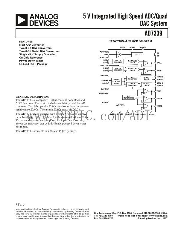
The AD7339 is an advanced composite integrated circuit designed for comprehensive data acquisition and signal processing tasks. Combining multiple functionalities, it features both an 8-bit Analog-to-Digital Converter (ADC) and a highly versatile array of two parallel and two serial Digital-to-Analog Converters (DACs)—all operating on a single power supply. This chip includes an integrated bandgap reference voltage and offers individual power-down capability across all sections, optimizing efficiency. It is ideal for engineers designing robust test equipment or measurement systems that require high precision in simultaneous analog conversion while minimizing power consumption.
Page 1 Text Content
5 V Integrated High Speed ADC/Quad
DAC System AD7339
FEATURES FUNCTIONAL BLOCK DIAGRAM
8-Bit A/D Converter
DVDD1 DGND1 AGND1
Two 8-Bit D/A Converters Two 8-Bit Serial D/A Converters ADCPDB
Single +5 V Supply Operation AIN T/H ADC
On-Chip Reference ADCCLK DA0 DAC A
Power-Down Mode PARALLEL
DA7 REGISTER DAC A DACA
52-Lead PQFP Package
DACCLK DB0 DAC B PARALLEL
REGISTER DAC B DACB
DACPDB
DAC 0 SERIAL SDAC0F
REGISTER DAC 0 SDAC0S
SERIAL
SDATA
CONTROL
SCLK LOGIC DAC 1 SDAC1F
SERIAL
REGISTER DAC 1 SDAC1S
LATCH
SDACPDB
GENERAL DESCRIPTION
REFERENCE
VREFA
The AD7339 is a composite IC that contains both DAC and
ADC functions. The device includes an 8-bit parallel A-to-D
AD7339
converter. Two 8-bit parallel DACs are also included as are two VREFB
serial control DACs. These serial DACs are 8-bit DACs.
The AD7339, which operates with a single 5 V power supply, DVDD2 DVDD3 DGND2 DGND3 AGND2 AGND3
has a bandgap reference on board with a nominal value of 2.5 V.
w.BDTIC.com/ADI To reduce the power consumption of the part, each section, except the reference, can be individually powered down when
not in use. The AD7339 is available in a 52-lead PQFP package.
REV. Information furnished by Analog Devices is believed to be accurate and reliable. However, no responsibility is assumed by Analog Devices for its
One Technology Way, P.O. Box 9106, Norwood, MA 02062-9106, U.S.A.
use, nor for any infringements of patents or other rights of third parties
which may result from its use. No license is granted by implication or Tel: 781/329-4700 World Wide Web Site: http://www.analog.com otherwise under any patent or patent rights of Analog Devices. Fax: 781/326-8703 © Analog Devices, Inc., 1997
Page Summary Contents For AD7339 Analog Devices Data Sheet
Manual Details
| Brand | Analog Devices |
|---|---|
| Pages | 12 |
| File Size | 152.87 KB |
| Published | May 14, 2026 |
Enter the captcha to get the download link:
