# A B C D E F G H I J K L M N O P Q R S T U V W X Y Z

ANALOG DEVICES AD9861 Data Sheet

Summary

The AD9861 is a high-performance, low-power bidirectional transceiver designed for demanding communications applications in the broadband market. This integrated converter features dual 10-bit ADCs (up to 80 MSPS) and TxDACs (up to 200 MSPS), supporting both full-duplex and half-duplex data transfer modes. The manual provides comprehensive details on the device's architecture, including specifications for the Rx Path, Tx Path, programmable configuration using SPI/mode pins, and power management. It is the ideal solution for engineering compact, cost-effective systems such as modems and broadband LAN access points.
📄 Preview 📖 Table of Contents Contents PAGE OF 52

Page 1 Text Content

Mixed-Signal Front-End (Mx FE™) Baseband Transceiver for Broadband Applications

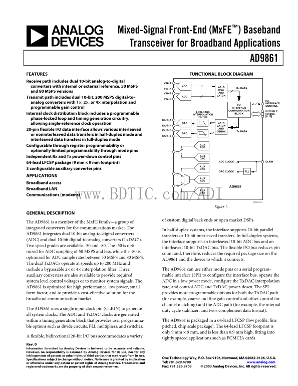
AD9861 FEATURES FUNCTIONAL BLOCK DIAGRAM Receive path includes dual 10-bit analog-to-digital

VIN+A

converters with internal or external reference, 50 MSPS ADC DATA

VIN–A Rx DATA

and 80 MSPS versions AND

VIN+B

LATCH

Transmit path includes dual 10-bit, 200 MSPS digital-to-

VIN–B

analog converters with 1×, 2×, or 4× interpolation and INTERFACE

CONTROL

programmable gain control INTERFACE CONFIGURATION FLEXIBLE

LOW-PASS

Internal clock distribution block includes a programmable INTERPOLATION BLOCK I/O BUS

FILTER [0:19]

phase-locked loop and timing generation circuitry,

IOUT+A

DAC DATA

allowing single-reference clock operation

IOUT–A LATCH

20-pin flexible I/O data interface allows various interleaved IOUT+B

DEMUX Tx DATA

or noninterleaved data transfers in half-duplex mode and IOUT–B interleaved data transfers in full-duplex mode

Configurable through register programmability or

optionally limited programmability through mode pins

Independent Rx and Tx power-down control pins AUX DAC

CLKINADC CLOCK

64-lead LFCSP package (9 mm × 9 mm footprint)

AUX 3 configurable auxiliary converter pins DAC

DAC CLOCK PLL

APPLICATIONS

AUX ADC

Broadband access

AD9861

Broadband LAN

AUX DAC

Communications (modems)

www.BDTIC.com/ADI

Figure 1.

GENERAL DESCRIPTION

of custom digital back ends or open market DSPs.

The AD9861 is a member of the Mx FE family—a group of integrated converters for the communications market. The

In half-duplex systems, the interface supports 20-bit parallel

AD9861 integrates dual 10-bit analog-to-digital converters

transfers or 10-bit interleaved transfers. In full-duplex systems,

(ADC) and dual 10-bit digital-to-analog converters (Tx DAC®).

the interface supports an interleaved 10-bit ADC bus and an

Two speed grades are available, -50 and -80. The -50 is opti-

interleaved 10-bit Tx DAC bus. The flexible I/O bus reduces pin

mized for ADC sampling of 50 MSPS and less, while the -80 is

count and, therefore, reduces the required package size on the

optimized for ADC sample rates between 50 MSPS and 80 MSPS.

AD9861 and the device to which it connects.

The dual Tx DACs operate at speeds up to 200 MHz and

include a bypassable 2× or 4× interpolation filter. Three The AD9861 can use either mode pins or a serial program- auxiliary converters are also available to provide required mable interface (SPI) to configure the interface bus, operate the system level control voltages or to monitor system signals. The ADC in a low power mode, configure the Tx DAC interpolation AD9861 is optimized for high performance, low power, small rate, and control ADC and Tx DAC power-down. The SPI form factor, and to provide a cost-effective solution for the provides more programmable options for both the Tx DAC path broadband communication market. (for example, coarse and fine gain control and offset control for channel matching) and the ADC path (for example, the internal

The AD9861 uses a single input clock pin (CLKIN) to generate

duty cycle stabilizer, and twos complement data format).

all system clocks. The ADC and Tx DAC clocks are generated

within a timing generation block that provides user programma- The AD9861 is packaged in a 64-lead LFCSP (low profile, fine ble options such as divide circuits, PLL multipliers, and switches. pitched, chip scale package). The 64-lead LFCSP footprint is only 9 mm × 9 mm, and is less than 0.9 mm high, fitting into

A flexible, bidirectional 20-bit I/O bus accommodates a variety

tightly spaced applications such as PCMCIA cards

Rev. 0 Information furnished by Analog Devices is believed to be accurate and reliable. However, no responsibility is assumed by Analog Devices for its use, nor for any infringements of patents or other rights of third parties that may result from its use.

One Technology Way, P.O. Box 9106, Norwood, MA 02062-9106, U.S.A.

Specifications subject to change without notice. No license is granted by implication

or otherwise under any patent or patent rights of Analog Devices. Trademarks and Tel: 781.329.4700 www.analog.com registered trademarks are the property of their respective owners. Fax: 781.326.8703 © 2003 Analog Devices, Inc. All rights reserved.

Page Summary Contents For ANALOG DEVICES AD9861 Data Sheet

Page 1 Mixed-Signal Front-End (Mx FE™) Baseband Transceiver for Broadband Applications AD9861 FEATURES FUNCTIONAL BLOCK DIAGRAM Receive path includes dual 10-bit analog-to-digital VIN+A converters with inter...
Page 2 AD9861 TABLE OF CONTENTS Tx Path Specifications...................................................................... Theory of Operation Rx Path Specifications...........................................
Page 3 AD9861 Tx PATH SPECIFICATIONS Table 1. AD9861-50 and AD9861-80 FDAC = 200 MSPS; 4× interpolation; RSET = 4.02 kΩ; differential load resistance of 100 Ω1; Tx PGA = 20 d B, AVDD = DVDD = 3.3 V, unless o...
Page 4 AD9861 Rx PATH SPECIFICATIONS Table 2. AD9861-50 and AD9861-80 FADC = 50 MSPS for the AD9861-50, 80 MSPS for the AD9861-80; internal reference; differential analog inputs, ADC_AVDD = DVDD = 3.3V, unle...
Page 5 AD9861 POWER SPECIFICATIONS Table 3. AD9861-50 and AD9861-80 Analog and digital supplies = 3.3 V; FCLKIN = 50 MHz; PLL 4× setting; normal timing mode Parameter Temp Test Level Min Typ Max Unit POWER S...
Page 6 AD9861 TIMING SPECIFICATIONS Table 5. AD9861-50 and AD9861-80 Parameter Temp Test Level Min Typ Max Unit INPUT CLOCK CLKIN Clock Rate (PLL Bypassed) Full IV 1 200 MHz PLL Input Frequency Full IV 16 20...
Page 7 AD9861 ABSOLUTE MAXIMUM RATINGS Table 7. Thermal Resistance Parameter Rating Electrical 64-lead LFCSP (4-layer board): AVDD Voltage 3.9 V max θJA = 24.2 (paddle soldered to ground plan, 0 LPM Air) DRV...
Page 8 AD9861 PIN CONFIGURATION AND PIN FUNCTION DESCRIPTIONS SPI_DIO CLKIN48 SPI_CLK AUXADC_REF47 SPI_SDO/AUX_SPI_SDO RESET46 ADC_LO_PWR/AUX_SPI_CS AUX_DACC/AUX_ADCB45 DVDD L044 DVSS L143 AVDD AD9861 L242 T...
Page 9 AD9861 Pin No. Name1 Description2, 3 34 AUX_SPI_CLK CLK for Aux SPI. 35–44 L9–L0 Lower Data Bit 9 to Lower Data Bit 0. 45 AUX3 Configurable as either Aux ADC_B or Aux DAC_C. 46 RESET Chip Reset When L...
Page 10 AD9861 PL IT (d FS PL IT (d FS PL IT (d FS TYPICAL PERFORMANCE CHARACTERISTICS FREQUENCY (MHz) 6- 0- 6- 0- FREQUENCY (MHz) 6- 0- Figure 4. AD9861-50 Rx Path Single-Tone FFT of Rx Channel B Path Figure...
Page 11 AD9861 SF (d c) SN (d c) PL IT (d FS FREQUENCY (MHz) FREQUENCY (MHz) Figure 10. AD9861-50 Rx Path Single-Tone FFT of Rx Channel B Path Figure 13. AD9861-50 Rx Path Dual-Tone FFT of Rx Channel A Path D...
Page 12 TH (d c) SN (d c) SN (d c) AD9861 IDEAL SNR INPUT AMPLITUDE (d BFS) INPUT AMPLITUDE (d BFS) Figure 16. AD9861-50 Rx Path at 50 MSPS, 10 MHz Input Tone Figure 19. AD9861-50 Rx Path at 50 MSPS, 10 MHz I...
Page 13 AD9861 PL IT (d FS PL IT (d FS PL IT (d FS FREQUENCY (MHz) FREQUENCY (MHz) Figure 22. AD9861-80 Rx Path Single-Tone FFT of Rx Channel B Path Figure 25. AD9861-80 Rx Path Dual-Tone FFT of Rx Channel A ...
Page 14 AD9861 SN (d c) SF (d c) SN (d c) LOW POWER ADC @ 40MSPS LOW POWER ADC @ 40MSPS ULTRALOW POWER ADC @ 16MSPS 9.8 ULTRALOW POWER ADC @ 16MSPS NORMAL POWER @ 80MSPS INPUT FREQUENCY (MHz) INPUT FREQUENCY ...
Page 15 AD9861 VD EN (m TH (d c) SN (d c) AVE (+85°C) AVE (–40°C) AVE (+85°C) 9.6 AVE (+25°C) AVE (+25°C) AVE (–40°C) ADC_AVDD VOLTAGE (V) ADC_AVDD VOLTAGE (V) Figure 34. AD9861-80 Rx Path at 80 MSPS, 10 MHz ...
Page 16 AD9861 PL IT (d c) PL IT (d c) PL IT (d c) FREQUENCY (MHz) FREQUENCY (MHz) Figure 40. AD9861 Tx Path 1 MHz Single-Tone Output FFT of Tx Path Figure 43. AD9861 Tx Path 5 MHz Single-Tone Output FFT of T...
Page 17 AD9861 IM (d c) SI (d c) TH (d c) OUTPUT FREQUENCY (MHz) OUTPUT FREQUENCY (MHz) Figure 46. AD9861 Tx Path THD vs. Output Frequency of Tx Path with Figure 49. AD9861 Tx Path THD vs. Output Frequency of...
Page 18 AD9861 PL IT (d c) PL IT (d c) PL IT (d c) Figure 52 to Figure 57 use the same input data to the Tx path, a 64-carrier OFDM signal over a 20 MHz bandwidth, centered at 20 MHz. The center two carriers ...
Page 19 AD9861 PL IT (d c) PL IT (d c) PL IT (d c) Figure 58 to Figure 63 use the same input data to the Tx path, a 256-carrier OFDM signal over a 1.75 MHz bandwidth, centered at 7 MHz. The center four carrie...
Page 20 AD9861 PL IT (d c) PL IT (d c) PL IT (d c) Figure 64 to Figure 69 use the same input data to the Tx path, a 256-carrier OFDM signal over a 23 MHz bandwidth, centered at 23 MHz. The center four carrier...
Page 21 AD9861 TERMINOLOGY Input Bandwidth Harmonic Distortion, Second The analog input frequency at which the spectral power of the The ratio of the rms signal amplitude to the rms value of the fundamental f...
Page 22 AD9861 THEORY OF OPERATION SYSTEM BLOCK The AD9861 is targeted to cover the mixed-signal front end The differential input stage is dc self-biased and allows needs of multiple wireless communication sy...
Page 23 AD9861 Rx Path Application Section default 1 V VREF reference accepts a 2 V p-p differential input swing and the offset voltage should be Adding series resistance between the output of the signal sour...
Page 24 AD9861 degradation in SNR at a given full-scale input frequency (f INPUT), 3, 4, and 5. Under this condition, the internal references are due only to aperture jitter (t A), can be calculated with the ...
Page 25 AD9861 DAC Equivalent Circuits REFERENCE DAC A AND DAC B The AD9861 Tx path consisting of dual 10-bit DACs is shown REFERENCE BIASES in Figure 73. The DACs integrate a high performance Tx DAC IOUTFSMA...
Page 26 AD9861 Clock Input Configuration The sleep mode, when activated, turns off the DAC output The quality of the clock and data input signals is important in currents, but the rest of the chip remains fun...
Page 27 AD9861 Update C, B, and A]. Slave mode is enabled by writing a high to AUXILIARY CONVERTERS the slave mode register bit [Register 0x28, Bit 7, Slave Enable]. The AD9861 contains auxiliary analog-to-di...
Page 28 AD9861 Table 10. Configuring Aux ADC Reference Refsel A/B Aux ADC_A Reference Aux ADC Ref Enable Aux ADC Ref FS [Register 0x22, Configuration [Register 0x17, Bit 1] [Register 0x17, Bit 0] Bit 2/Bit 5]...
Page 29 AD9861 Figure 76 shows a timing diagram of the Aux SPI when it is used to control and access an Aux ADC. Figure 77 shows the timing for each of the three Aux ADC modes of operation. AUXSPI_CS AUXSPI_C...
Page 30 AD9861 Flexible I/O Interface Options DIGITAL BLOCK The AD9861 can accommodate various data interface transfer The AD9861 digital block allows the device to be configured in options (flexible I/O). Th...
Page 31 AD9861 Table 12 describes AD9861 pin function (when mode pins are used) relative to I/O mode, and for half-duplex modes whether transmitting or receiving. Table 12. AD9861 Pin Function vs. Interface M...
Page 32 AD9861 • Buffered Tx clock output (from IFACE3 pin) equals 2× the • Max ADC sampling rate = 50 MSPS (AD9861-50) or DAC update rate; one rising edge per interleaved Tx sample. 80 MSPS (AD9861-80). Note...
Page 33 AD9861 mode. Both the U10 and L10 buses are used on the AD9861. • Max ADC sampling rate = 50 MSPS (AD9861-50) or The logic level of the Tx/Rx selector (controlled through the 80 MSPS (AD9861-80). IFAC...
Page 34 AD9861 Table 15. Mode Pin Names and Descriptions Pin Name Description ADC_LO_PWR ADC Low Power Mode Option. ADC_LO_PWR is latched during the rising edge of RESET. Logic low results in ADC operation at...
Page 35 AD9861 Configuring with SPI The flexible interface can be configured with register settings. Using the register allows more device programmability. Table 16 shows the required register writes to confi...
Page 36 AD9861 SPI Register Map Registers 0x00 to 0x29 of the AD9861 provide flexible operation of the device. The SPI allows access to many configurable options. Detailed descriptions of the bit functions ar...
Page 37 AD9861 Table 18. Register Bit Descriptions Register Bit Description Register 0: General Bit 7: SDIO Bi Dir (Bidirectional) Default setting is low, which indicates that the SPI serial port uses dedicat...
Page 38 AD9861 Register Bit Description Bit 6: Rx REF (Power-Down) Setting this register bit high powers down internal ADC reference circuits. Powering down these circuits provides additional power saving ove...
Page 39 AD9861 Register Bit Description Bit 4: Tx PGA Fast Update (Mode) The Tx PGA fast bit controls the update speed of the Tx PGA. When fast update mode is enabled, the Tx PGA provides fast gain settling w...
Page 40 AD9861 Register Bit Description Register 17: Auxiliary Converters Bits 7–2: Aux DAC A FS/Aux DAC B These register bits independently scale the full-scale output voltage for the Aux DACs. If the full- ...

Manual Details

Brand Analog Devices
Pages 52
File Size 1.00 MB
Published May 14, 2026
180 views

Enter the captcha to get the download link:

captcha

Frequently Asked Questions

What ADC sample rates are available?

The AD9861 is optimized for ADC sampling of 50 MSPS and less (for the -50 grade), or between 50 MSPS and 80 MSPS (for the -80 grade).

Does the device support full-duplex communication?

Yes, in full-duplex systems, the interface supports an interleaved 10-bit ADC bus and an optimized TxDAC bus.

How can I program or configure the AD9861?

It can be configured using a serial program-programmable interface (SPI) or via mode pins if no SPI is available.

What are the two speed grades advertised?

Two speeds grades, -50 and -80, are available, both packaged in a 64-lead LFCSP (CP-64).