AD7683 ANALOG DEVICES Data Manual
Summary
This high-performance 16-bit Analog-to-Digital Converter (ADC) delivers a reliable 100 kSPS throughput for demanding single-supply applications. Suitable for data acquisition, medical instruments, and process control requiring accurate measurements in portable or battery-powered systems. Operators will find comprehensive guidance within this manual, covering detailed specifications, analog input architectures, SPI interface configurations, and performance evaluation methods to ensure seamless integration of this powerful component into their designs.
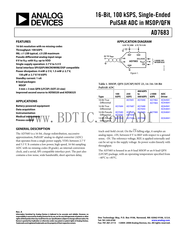
Page 1 Text Content
16-Bit, 100 k SPS, Single-Ended Pul SAR ADC in MSOP/QFN
AD7683 FEATURES APPLICATION DIAGRAM
0.5V TO VDD 2.7V TO 5.5V
16-bit resolution with no missing codes Throughput: 100 k SPS INL: ±1 LSB typical, ±3 LSB maximum
REF VDD
0V TO VREF
Pseudo differential analog input range
+IN DCLOCK
0 V to VREF with VREF up to VDD 3-WIRE SPI
–IN AD7683 DOUT
INTERFACE
Single-supply operation: 2.7 V to 5.5 V CS
Serial interface SPI/QSPI/MICROWIRE/DSP compatible Power dissipation: 4 m W @ 5 V, 1.5 m W @ 2.7 V,
Figure 1.
150 μW @ 2.7 V/10 k SPS Standby current: 1 n A 8-lead packages:
Table 1. MSOP, QFN (LFCSP)/SOT-23, 14-/16-/18-Bit
Pul SAR ADC
3 mm × 3 mm QFN (LFCSP) (SOT-23 size)
400 k SPS
Improved second source to ADS8320 and ADS8325
to ≥1000 ADC
Type k SPS k SPS 500 k SPS k SPS Driver
18-Bit True AD7691 AD7690 AD7982 ADA4941
APPLICATIONS
Differential AD7984 ADA4841
Battery-powered equipment 16-Bit True AD7684 AD7687 AD7688 ADA4941
Data acquisition Differential AD7693 ADA4841 16-Bit Pseudo AD7680 AD7686 AD7685 AD7980 ADA4841
Instrumentation
Differential AD7683 AD7694
Medical instruments
14-Bit Pseudo AD7940 AD7942 AD7946 ADA4841
Process control www.BDTIC.com/ADI
Differential
GENERAL DESCRIPTION
track-and-hold circuit. On the CS falling edge, it samples an
The AD7683 is a 16-bit, charge redistribution, successive
analog input, +IN, between 0 V to REF with respect to a ground
approximation, Pul SAR® analog-to-digital converter (ADC)
sense, –IN. The reference voltage, REF, is applied externally and
that operates from a single power supply, VDD, between 2.7 V
can be set up to the supply voltage. Its power scales linearly with
and 5.5 V. It contains a low power, high speed, 16-bit sampling
throughput.
ADC with no missing codes (B grade), an internal conversion
The AD7683 is housed in an 8-lead MSOP or an 8-lead QFN
clock, and a serial, SPI-compatible interface port. The part also
(LFCSP) package, with an operating temperature specified from
contains a low noise, wide bandwidth, short aperture delay,
−40°C to +85°C.
Rev. A Information furnished by Analog Devices is believed to be accurate and reliable. However, no responsibility is assumed by Analog Devices for its use, nor for any infringements of patents or other
One Technology Way, P.O. Box 9106, Norwood, MA 02062-9106, U.S.A.
rights of third parties that may result from its use. Specifications subject to change without notice. No
license is granted by implication or otherwise under any patent or patent rights of Analog Devices. Tel: 781.329.4700 www.analog.com Trademarks and registered trademarks are the property of their respective owners. Fax: 781.461.3113 ©2004–2008 Analog Devices, Inc. All rights reserved.
Page Summary Contents For AD7683 ANALOG DEVICES Data Manual
Manual Details
| Brand | Analog Devices |
|---|---|
| Pages | 16 |
| File Size | 398.58 KB |
| Published | May 14, 2026 |
Enter the captcha to get the download link:

Frequently Asked Questions
What input range does the AD7683 support?
The analog input range is pseudo differential, with +IN ranging from 0V to REF and –IN ranging between 0V and VREF.
How is power consumption related to operating conditions?
Power dissipation scales linearly with supply voltage (VDD), such as being 4 mW @ 5 V or 1.5 mW @ 2.7 V.
Is the AD7683 compatible with different interfaces and supply voltages?
Yes, it supports single-supply operation from 2.7V to 5.5V and features a serial, SPI-compatible interface (SPI/QSPI/MICROWIRE/DSP).
What is the operating temperature range for the device?
The typical operating temperature specification range for this part is listed as –40°C to +85°C.