AD5066 Analog Devices Data Handbook/Manual
Summary
The AD5066 is a high-performance, low power quad 16-bit unbuffered DAC ideal for demanding applications like data acquisition and process control. Featuring industry-leading accuracy (±1 LSB INL) and operating from 2.7 V to 5.5 V, this device offers fast settling times and robust power management features. This summary provides a comprehensive overview of the AD5066's technical specifications, high-speed operation details, functionality, and application guidelines for engineers selecting precise digital signal components.
Page 1 Text Content
Fully Accurate 16-Bit Un Buffered VOUT DAC SPI
Interface 2.7 V to 5.5 V in a TSSOP
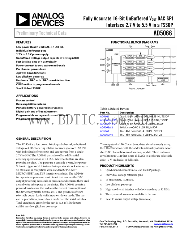
Preliminary Technical Data AD5066 FEATURES FUNCTIONAL BLOCK DIAGRAMS Low power Quad 16 bit DAC, ± 1LSB INL Individual reference pins 2.7 V to 5.5 V power supply Unbuffered voltage output capable of driving 60KΩ Fast Settling time of 4 us typically Power-on reset to zero scale or mid-scale Per channel power-down 3 power-down functions Low glitch on power up Hardware LDAC with LDAC override function CLR Function to programmable code Small 16 lead TSSOP Figure 1.AD5066
APPLICATIONS Process control Data acquisition systems Portable battery-powered instruments
Table 1. Related Devices
Digital gain and offset adjustment
Part No. Description
Programmable voltage and current sources
AD5666 Quad,16-bit buffered D/A,16 LSB INL, TSSOP
Programmable attenuators
AD5065/45/25 Quad,16-bit buffered D/A,1 LSB INL, TSSOP
www.BDTIC.com/A AD5064/44/24 Quad 16-bit nano DAC, 1 LSB INL, TSSOP
AD5063/62 16-bit nano DAC, 1 LSB INL, MSOP AD5061 16-/14bit nano DAC, 4 LSB INL, SOT-23 AD5060/40 16-/14bit nano DAC, 1 LSB INL, SOT-23
GENERAL DESCRIPTION The AD5066 is a low power, 16-bit quad-channel, unbuffered The outputs of all DACs can be updated simultaneously using
voltage-out DAC offering relative accuracy specs of 1LSB INL the LDAC function, with the added functionality of user-select-
with individual reference pin and can operate from a single able DAC channels to simultaneously update. There is also an 2.7V to 5.5V. The AD5066 parts also offer a differential asynchronous CLR that clears all DACs to a software-selectable accuracy specification of ±1 LSB. Reference buffers are also
code - 0 V, midscale, or full scale.
provided on-chip. The parts use a versatile 3-wire, low power
Schmitt trigger serial interface that operates at clock rates up to PRODUCT HIGHLIGHTS
50 MHz and is compatible with standard SPI®, QSPI™, 1. Quad channel available in 16-lead TSSOP package. MICROWIRE™, and DSP interface standards. The AD5066
2. Individual voltage reference pins
incorporates a power-on reset circuit that ensures the DAC
3. 16 bit accurate, 1 LSB INL.
output powers up zero scale or midscale and remains there until
a valid write takes place to the device. The AD5066 contain a 4. Low glitch on power-up.
power-down feature that reduces the current consumption of
5. High speed serial interface with clock speeds up to 50 MHz.
the device to typically 330 n A at 5 V and provides software
6. Three power-down modes available to the user.
selectable output loads while in power-down mode. The part
can be placed into power-down mode over the serial interface. 7. Reset to known output voltage (zero scale).
Total unadjusted error for the part is <0.8 m V. Both parts exhibit very low glitch on power-up.
Rev. Pr B Information furnished by Analog Devices is believed to be accurate and reliable. However, no responsibility is assumed by Analog Devices for its use, nor for any infringements of patents or other
One Technology Way, P.O. Box 9106, Norwood, MA 02062-9106, U.S.A.
rights of third parties that may result from its use. Specifications subject to change without notice. No
license is granted by implication or otherwise under any patent or patent rights of Analog Devices. Tel: 781.329.4700 www.analog.com Trademarks and registered trademarks are the property of their respective owners. Fax: 781.461.3113 © 2007 Analog Devices, Inc. All rights reserved.
Page Summary Contents For AD5066 Analog Devices Data Handbook/Manual
Manual Details
| Brand | Analog Devices |
|---|---|
| Pages | 20 |
| File Size | 441.51 KB |
| Published | May 14, 2026 |
Enter the captcha to get the download link:

Frequently Asked Questions
What is the maximum clock speed for the AD5066 interface?
The high-speed serial interface operates at clock rates up to 50 MHz, supporting standards like SPI®, QSPI™, and MICROWIRE cloud.
How does the device behave when powered on or reset?
It powers up either to the zero scale or midscale and has a power-on reset circuit that ensures low glitch on startup. It can be cleared asynchronously to any code.
What is the required operating voltage range for AD5066?
The device operates using a power supply voltage (VDD) ranging from 2.7 V to 5.5 V.
Are there methods to reduce power consumption?
Yes, the AD5066 offers three distinct power-down modes available to the user for reducing current draw.
What is the guaranteed resolution and accuracy of the DAC?
The device features 16-bit resolution with a relative accuracy specification of ±1 LSB INL.