ALTERA Cyclone III Device Family Pin Connection Guidelines Manual
Summary
Essential guidelines for connecting programmable logic devices within the Cyclone III family. This manual provides critical information on proper pin assignment, covering internal voltage standards (VCCINT), high-speed differential interfaces, and external memory connectivity. It is designed for hardware engineers and designers utilizing Altera Cyclone III FPGAs to ensure optimal device operation and reliable system design through preliminary connection recommendations.
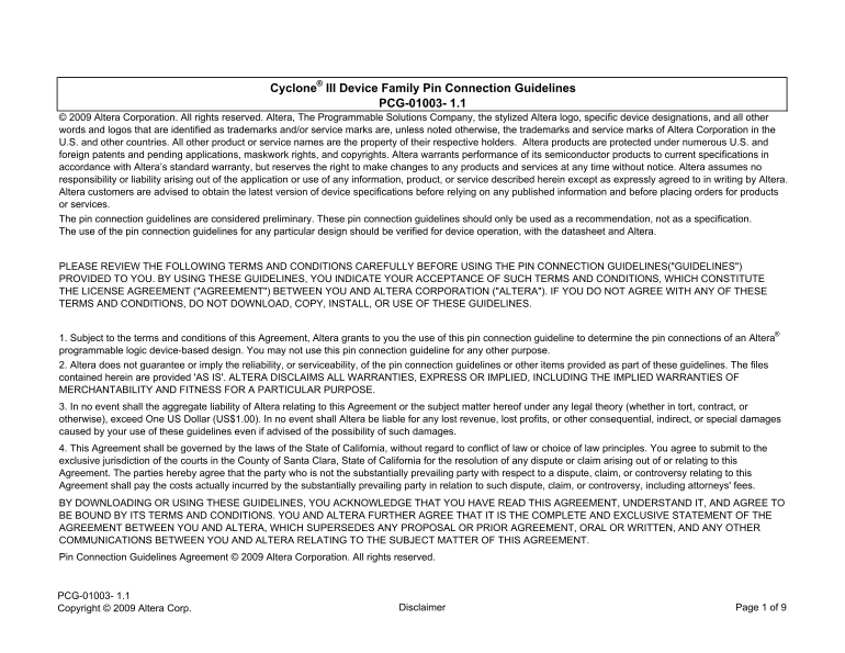
Page 1 Text Content
Cyclone® III Device Family Pin Connection Guidelines
PCG-01003- 1.1
© 2009 Altera Corporation. All rights reserved. Altera, The Programmable Solutions Company, the stylized Altera logo, specific device designations, and all other words and logos that are identified as trademarks and/or service marks are, unless noted otherwise, the trademarks and service marks of Altera Corporation in the U.S. and other countries. All other product or service names are the property of their respective holders. Altera products are protected under numerous U.S. and foreign patents and pending applications, maskwork rights, and copyrights. Altera warrants performance of its semiconductor products to current specifications in accordance with Altera’s standard warranty, but reserves the right to make changes to any products and services at any time without notice. Altera assumes no responsibility or liability arising out of the application or use of any information, product, or service described herein except as expressly agreed to in writing by Altera. Altera customers are advised to obtain the latest version of device specifications before relying on any published information and before placing orders for products or services. The pin connection guidelines are considered preliminary. These pin connection guidelines should only be used as a recommendation, not as a specification. The use of the pin connection guidelines for any particular design should be verified for device operation, with the datasheet and Altera.
PLEASE REVIEW THE FOLLOWING TERMS AND CONDITIONS CAREFULLY BEFORE USING THE PIN CONNECTION GUIDELINES("GUIDELINES") PROVIDED TO YOU. BY USING THESE GUIDELINES, YOU INDICATE YOUR ACCEPTANCE OF SUCH TERMS AND CONDITIONS, WHICH CONSTITUTE THE LICENSE AGREEMENT ("AGREEMENT") BETWEEN YOU AND ALTERA CORPORATION ("ALTERA"). IF YOU DO NOT AGREE WITH ANY OF THESE TERMS AND CONDITIONS, DO NOT DOWNLOAD, COPY, INSTALL, OR USE OF THESE GUIDELINES.
1. Subject to the terms and conditions of this Agreement, Altera grants to you the use of this pin connection guideline to determine the pin connections of an Altera ® programmable logic device-based design. You may not use this pin connection guideline for any other purpose. 2. Altera does not guarantee or imply the reliability, or serviceability, of the pin connection guidelines or other items provided as part of these guidelines. The files contained herein are provided 'AS IS'. ALTERA DISCLAIMS ALL WARRANTIES, EXPRESS OR IMPLIED, INCLUDING THE IMPLIED WARRANTIES OF MERCHANTABILITY AND FITNESS FOR A PARTICULAR PURPOSE. 3. In no event shall the aggregate liability of Altera relating to this Agreement or the subject matter hereof under any legal theory (whether in tort, contract, or otherwise), exceed One US Dollar (US$1.00). In no event shall Altera be liable for any lost revenue, lost profits, or other consequential, indirect, or special damages caused by your use of these guidelines even if advised of the possibility of such damages. 4. This Agreement shall be governed by the laws of the State of California, without regard to conflict of law or choice of law principles. You agree to submit to the exclusive jurisdiction of the courts in the County of Santa Clara, State of California for the resolution of any dispute or claim arising out of or relating to this Agreement. The parties hereby agree that the party who is not the substantially prevailing party with respect to a dispute, claim, or controversy relating to this Agreement shall pay the costs actually incurred by the substantially prevailing party in relation to such dispute, claim, or controversy, including attorneys' fees. BY DOWNLOADING OR USING THESE GUIDELINES, YOU ACKNOWLEDGE THAT YOU HAVE READ THIS AGREEMENT, UNDERSTAND IT, AND AGREE TO BE BOUND BY ITS TERMS AND CONDITIONS. YOU AND ALTERA FURTHER AGREE THAT IT IS THE COMPLETE AND EXCLUSIVE STATEMENT OF THE AGREEMENT BETWEEN YOU AND ALTERA, WHICH SUPERSEDES ANY PROPOSAL OR PRIOR AGREEMENT, ORAL OR WRITTEN, AND ANY OTHER COMMUNICATIONS BETWEEN YOU AND ALTERA RELATING TO THE SUBJECT MATTER OF THIS AGREEMENT. Pin Connection Guidelines Agreement © 2009 Altera Corporation. All rights reserved.
PCG-01003- 1.1
Copyright © 2009 Altera Corp. Disclaimer Page 1 of 9
Page Summary Contents For ALTERA Cyclone III Device Family Pin Connection Guidelines Manual
Manual Details
| Brand | CyClone |
|---|---|
| Pages | 9 |
| File Size | 186.45 KB |
| Published | May 18, 2026 |
Enter the captcha to get the download link:

Frequently Asked Questions
Must I rely solely on these pin connection guidelines for my design?
No, the guidelines are only a recommendation and must be verified for operation using the datasheet and Altera.
What is the maximum AC voltage input for I/O inputs?
All I/O inputs must maintain a maximum AC voltage of 4.1 V.
How should I check my pin connections before use?
Create a Quartus II design, enter your device I/O assignments, and compile the design to ensure proper operation.
What is the liability limit regarding these guidelines?
Altera’s aggregate liability relating to this Agreement shall not exceed One US Dollar (US$1.00).