AD OP07D 150 μV Maximum Offset Voltage Op Amp Data Sheet User Manual
Summary
The OP07D is a high-performance, ultralow offset precision operational amplifier designed for demanding industrial and medical instrumentation. Featuring an ultra-low offset voltage (150 μV max) and exceptional stability across wide temperature ranges (−40°C to +125°C), it is perfect for applications such as sensor interfaces, strain bridges, and precision filtering. This technical manual provides comprehensive documentation, including detailed electrical specifications, pin configurations, recommended application circuits, and operational parameters required by design engineers.
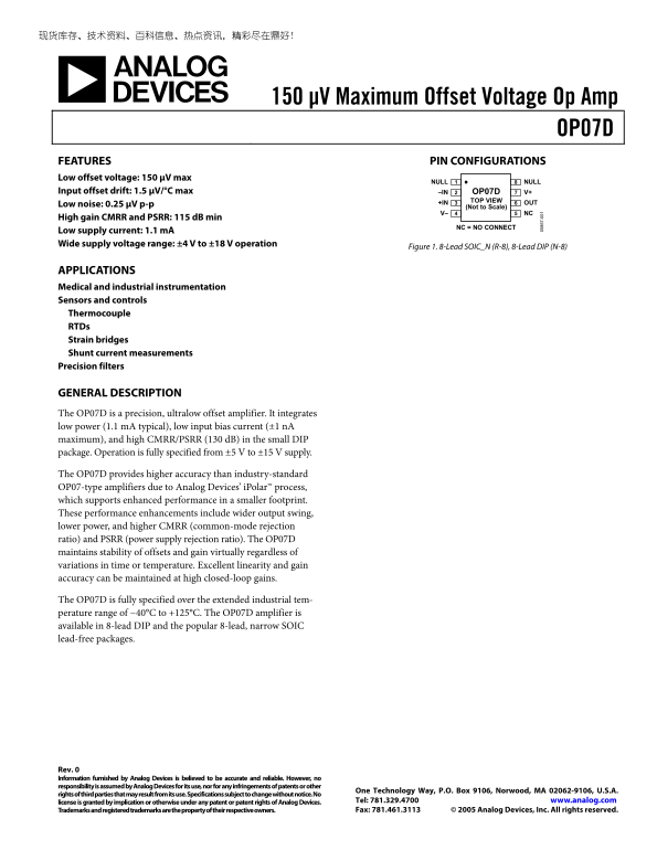
Page 1 Text Content
150 μV Maximum Offset Voltage Op Amp
OP07D FEATURES PIN CONFIGURATIONS Low offset voltage: 150 μV max
1NULL NULL
Input offset drift: 1.5 μV/°C max 2–IN OP07D V+
TOP VIEW Low noise: 0.25 μV p-p 3+IN OUT (Not to Scale) 4V– NC
High gain CMRR and PSRR: 115 d B min
NC = NO CONNECT
Low supply current: 1.1 m A Wide supply voltage range: ±4 V to ±18 V operation
Figure 1. 8-Lead SOIC_N (R-8), 8-Lead DIP (N-8)
APPLICATIONS Medical and industrial instrumentation Sensors and controls Thermocouple RTDs Strain bridges Shunt current measurements Precision filters
GENERAL DESCRIPTION The OP07D is a precision, ultralow offset amplifier. It integrates low power (1.1 m A typical), low input bias current (±1 n A maximum), and high CMRR/PSRR (130 d B) in the small DIP package. Operation is fully specified from ±5 V to ±15 V supply.
The OP07D provides higher accuracy than industry-standard OP07-type amplifiers due to Analog Devices’ i Polar™ process, which supports enhanced performance in a smaller footprint. These performance enhancements include wider output swing, lower power, and higher CMRR (common-mode rejection ratio) and PSRR (power supply rejection ratio). The OP07D 7- maintains stability of offsets and gain virtually regardless of variations in time or temperature. Excellent linearity and gain accuracy can be maintained at high closed-loop gains.
The OP07D is fully specified over the extended industrial tem- perature range of −40°C to +125°C. The OP07D amplifier is available in 8-lead DIP and the popular 8-lead, narrow SOIC lead-free packages.
Rev. 0 Information furnished by Analog Devices is believed to be accurate and reliable. However, no responsibility is assumed by Analog Devices for its use, nor for any infringements of patents or other
One Technology Way, P.O. Box 9106, Norwood, MA 02062-9106, U.S.A.
rights of third parties that may result from its use. Specifications subject to change without notice. No
license is granted by implication or otherwise under any patent or patent rights of Analog Devices. Tel: 781.329.4700 www.analog.com Trademarks and registered trademarks are the property of their respective owners. Fax: 781.461.3113 © 2005 Analog Devices, Inc. All rights reserved.
Page Summary Contents For AD OP07D 150 μV Maximum Offset Voltage Op Amp Data Sheet User Manual
Manual Details
| Brand | Maximum |
|---|---|
| Pages | 16 |
| File Size | 256.14 KB |
| Published | May 29, 2026 |
Enter the captcha to get the download link:

Frequently Asked Questions
What temperature range can the OP07D operate in?
It operates over an extended industrial temperature range from −40°C to +125°C.
How does the performance of OP07D compare to standard OP07-type amplifiers?
OP07D provides higher accuracy due to iPolar™ process enhancements, including wider output swing and higher CMRR/PSRR.
What physical packages are available for this amplifier?
It is available in 8-lead DIP and the popular 8-lead, narrow SOIC lead-free packages.
What is the typical low power supply current draw?
The typical supply current when V = 0V is 1.1 mA.