National Semiconductor CLC415 Quad, Wideband Monolithic Op Amp Data Sheet
Summary
This datasheet provides comprehensive technical details for the CLC415 Quad Wideband Monolithic Operational Amplifier. Designed for demanding analog circuits, this high-performance op amp offers superior signal integrity and low power consumption across various applications, including HDTV distribution, video processing, and active filtering. The accompanying manual covers detailed electrical characteristics, wideband performance graphs (e.g., frequency response, settling time), packaging options (DIP/SOIC), and application guidelines, making it an essential resource for analog circuit designers and engineers in signal processing fields.
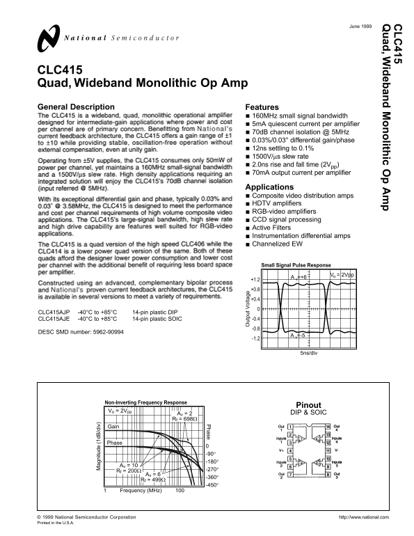
Page 1 Text Content
June 1999
ad ,W id eb an lith ic O
CLC415 Quad, Wideband Monolithic Op Amp ag ni tu de 1d /d iv General Description Features
160MHz small signal bandwidth 5m A quiescent current per amplifier 70d B channel isolation @ 5MHz 0.03%/0.03° differential gain/phase 12ns settling to 0.1% 1500V/µs slew rate 2.0ns rise and fall time (2Vpp) 70m A output current per amplifier
Applications Composite video distribution amps HDTV amplifiers
RGB-video amplifiers CCD signal processing Active Filters Instrumentation differential amps Channelized EW
ut pu t V ol ta ge
Small Signal Pulse Response
V = 2Vppo
CLC415AJP -40°C to +85°C 14-pin plastic DIP
CLC415AJE -40°C to +85°C 14-pin plastic SOIC -0.4 -0.8
DESC SMD number: 5962-90994
5ns/div
Non-Inverting Frequency Response
Pinout
Vo = 2Vpp
Av = 2 DIP & SOIC
Rf = 698Ω
Phase
Av = 10
Rf = 200Ω -270°
Av = 6
Rf = 499Ω
1 Frequency (MHz) 100
1999 National Semiconductor Corporation http://www.national.com Printed in the U.S.A.
Page Summary Contents For National Semiconductor CLC415 Quad, Wideband Monolithic Op Amp Data Sheet
Manual Details
| Brand | National |
|---|---|
| Pages | 6 |
| File Size | 338.71 KB |
| Published | June 17, 2026 |
Enter the captcha to get the download link:

Frequently Asked Questions
What is the maximum small signal bandwidth?
The product offers a small signal bandwidth of 160MHz.
Is this device suitable for critical life support applications?
No, National Semiconductor requires express written approval for use in life support devices or systems.
How much current can each amplifier output?
Each amplifier has an output current capability of up to 70mA.
What are the available operating temperature ranges?
Specific package options like CLC415AJP and CLC415AJE support temperatures from -40°C to +85°C.