National Semiconductor OP-07 Data Handbook Low Offset, Low Drift Operational Amplifier Manual
Summary
Engineered for high precision, the OP-07 operational amplifier delivers ultra-low offset voltage and exceptional drift stability in analog circuits. This versatile component operates across a wide supply range (3V–18V), making it ideal for sensitive instrumentation, scientific monitoring, and differential signal amplification. The accompanying manual provides detailed technical specifications, noise characteristics, gain models, and tailored application guides, serving electronics engineers who require high-accuracy performance in demanding measurement systems.
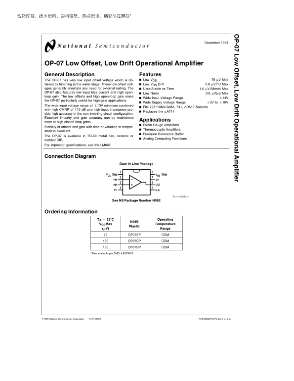
Page 1 Text Content
December
-0 ffs t, rift ra tio lifie OP-07 Low Offset, Low Drift Operational Amplifier General Description Features
The OP-07 has very low input offset voltage which is ob- Low VOS m V Max
tained by trimming at the wafer stage. These low offset volt- Low VOS Drift 0.6 m V/§C Max ages generally eliminate any need for external nulling. The Ultra-Stable vs Time 1.0 m V/Month Max OP-07 also features low input bias current and high open- Low Noise 0.6 m Vp-p Max loop gain. The low offsets and high open-loop gain make
Wide Input Voltage Range g14V
the OP-07 particularly useful for high-gain applications.
Wide Supply Voltage Range g3V to g18V
The wide input voltage range of g13V minimum combined
Fits 725/108A/308A, 741, AD510 Sockets
with high CMRR of d B and high input impedance pro-
Replaces the m A714
vide high accuracy in the non-inverting circuit configuration. Excellent linearity and gain accuracy can be maintained
Applications
even at high closed-loop gains.
Strain Gauge Amplifiers
Stability of offsets and gain with time or variation in temper-
Thermocouple Amplifiers
ature is excellent.
Precision Reference Buffer
The OP-07 is available in TO-99 metal can, ceramic or
Analog Computing Functions
molded DIP. For improved specifications, see the LM607.
Connection Diagram
Dual-In-Line Package
TL/H/10550–1
See NS Package Number N08E
Ordering Information
TA 25§C Operating
VOSMax Temperature
Plastic
(m V) Range
OP07EP COM
OP07CP COM
OP07DP COM *Also available per SMD Ý8203602
C1995 National Semiconductor Corporation TL/H/10550 RRD-B30M115/Printed in U. S. A.
Page Summary Contents For National Semiconductor OP-07 Data Handbook Low Offset, Low Drift Operational Amplifier Manual
Manual Details
| Brand | National |
|---|---|
| Pages | 6 |
| File Size | 141.56 KB |
| Published | May 27, 2026 |
Enter the captcha to get the download link:

Frequently Asked Questions
What is the maximum supply voltage range for the OP-07?
The device supports a wide supply voltage range from 3V up to 18V.
Does the OP-07 require external nulling for low offset voltages?
No, its low offsets generally eliminate any need for external nulling.
What is the minimum closed-loop bandwidth achievable with the OP-07?
The datasheet indicates a theoretical low range of 0.4 MHz for the closed-loop bandwidth (R2A and R2B are electronically trimmed).
How does the OP-07 perform in high-gain applications?
It is useful for high-gain applications because of its low offsets and high open-loop gain, while maintaining excellent linearity.