Vishay - TCDT1110 TCDT1110G Data Sheet User Manual
Summary
Achieve safe electrical isolation with this advanced optocoupler, designed for applications requiring separation from mains voltage sources. This device features a reliable transistor output and adheres to rigorous international safety standards (IEC/VDE). The accompanying manual provides comprehensive data on its performance parameters, absolute maximum ratings, and structural characteristics. It is essential for engineers developing high-safety electronics, power supplies, telecommunication gear, and household appliances where electrical shock protection is paramount.
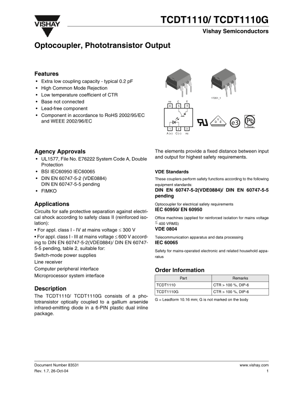
Page 1 Text Content
TCDT1110/ TCDT1110G
Vishay Semiconductors
Optocoupler, Phototransistor Output
Features Extra low coupling capacity - typical 0.2 p F High Common Mode Rejection Low temperature coefficient of CTR
Base not connected nc
Lead-free component Component in accordance to Ro HS 2002/95/EC and WEEE 2002/96/EC Pb
e3 Pb-free
(–) nc
Agency Approvals The elements provide a fixed distance between input and output for highest safety requirements.
UL1577, File No. E76222 System Code A, Double Protection BSI IEC60950 IEC60065 VDE Standards DIN EN 60747-5-2 (VDE0884) These couplers perform safety functions according to the following DIN EN 60747-5-5 pending equipment standards:
FIMKO DIN EN 60747-5-2(VDE0884)/ DIN EN 60747-5-5 pending Applications Optocoupler for electrical safety requirements IEC 60950/ EN 60950
Circuits for safe protective separation against electri- cal shock according to safety class II (reinforced iso- Office machines (applied for reinforced isolation for mains voltage
lation): ≤ 400 VRMS) • For appl. class I - IV at mains voltage ≤ 300 V VDE 0804
• For appl. class I - III at mains voltage ≤ 600 V accord- Telecommunication apparatus and data processing ing to DIN EN 60747-5-2(VDE0884)/ DIN EN 60747- IEC 60065 5-5 pending, table 2, suitable for:
Safety for mains-operated electronic and related household appa-
Switch-mode power supplies
ratus
Line receiver Computer peripheral interface
Order Information
Microprocessor system interface
Part Remarks
TCDT1110 CTR > 100 %, DIP-6
Description
TCDT1110G CTR > 100 %, DIP-6
The TCDT1110/ TCDT1110G consists of a pho-
G = Leadform 10.16 mm; G is not marked on the body
totransistor optically coupled to a gallium arsenide infrared-emitting diode in a 6-PIN plastic dual inline package.
Document Number 83531 www.vishay.com Rev. 1.7, 26-Oct-04
Page Summary Contents For Vishay - TCDT1110 TCDT1110G Data Sheet User Manual
Manual Details
| Brand | Vishay |
|---|---|
| Pages | 10 |
| File Size | 208.05 KB |
| Published | June 01, 2026 |
Enter the captcha to get the download link:

Frequently Asked Questions
What standards dictate the safety isolation of this device?
It complies with UL1577, BSI IEC60950, VDE Standards, ensuring safe protective separation against electrical shock.
What is the typical Current Transfer Ratio (CTR)?
The typical current transfer ratio (CTR) in this optocoupler is 100%.
What is the rated impulse voltage for safety?
The maximum safety rating includes a rated impulse voltage of 6kV.
What are the acceptable ambient and storage temperature ranges?
Ambient operation range is -55 to +100 °C, while storage can withstand temperatures from -55 to +125 °C.