Vishay TCDT1100 TCDT1100G Handbook
Summary
The TCDT1100G series provides robust phototransistor optocouplers designed for critical applications demanding reinforced electrical safety. These semiconductors ensure high levels of isolation up to 3750 V RMS, making them ideal for switch-mode power supplies, data processing, and mains-operated electronics. This manual offers a comprehensive guide to the device's characteristics, including detailed CTR variations and adherence to essential safety standards like VDE and UL, assisting engineers in designing reliable and electrically safe systems.
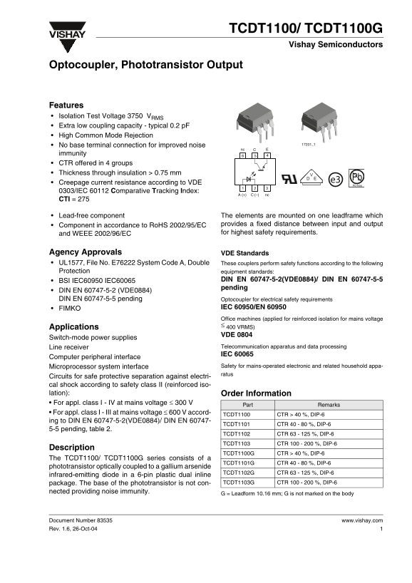
Page 1 Text Content
TCDT1100/ TCDT1100G
Vishay Semiconductors
Optocoupler, Phototransistor Output
Features Isolation Test Voltage 3750 VRMS Extra low coupling capacity - typical 0.2 p F High Common Mode Rejection
No base terminal connection for improved noise
immunity CTR offered in 4 groups Thickness through insulation > 0.75 mm
e3 Pb
Creepage current resistance according to VDE
Pb-free
0303/IEC 60112 Comparative Tracking Index:
(–) nc
CTI = 275
Lead-free component The elements are mounted on one leadframe which
Component in accordance to Ro HS 2002/95/EC provides a fixed distance between input and output and WEEE 2002/96/EC for highest safety requirements.
Agency Approvals VDE Standards UL1577, File No. E76222 System Code A, Double These couplers perform safety functions according to the following Protection equipment standards:
BSI IEC60950 IEC60065 DIN EN 60747-5-2(VDE0884)/ DIN EN 60747-5-5 pending
DIN EN 60747-5-2 (VDE0884) DIN EN 60747-5-5 pending Optocoupler for electrical safety requirements
FIMKO IEC 60950/EN 60950 Office machines (applied for reinforced isolation for mains voltage ≤ 400 VRMS)
Applications
VDE 0804
Switch-mode power supplies
Line receiver Telecommunication apparatus and data processing IEC 60065
Computer peripheral interface
Microprocessor system interface Safety for mains-operated electronic and related household appa- ratus
Circuits for safe protective separation against electri- cal shock according to safety class II (reinforced iso- lation): Order Information • For appl. class I - IV at mains voltage ≤ 300 V
Part Remarks
• For appl. class I - III at mains voltage ≤ 600 V accord-
TCDT1100 CTR > 40 %, DIP-6
ing to DIN EN 60747-5-2(VDE0884)/ DIN EN 60747-
TCDT1101 CTR 40 - 80 %, DIP-6
5-5 pending, table 2.
TCDT1102 CTR 63 - 125 %, DIP-6
TCDT1103 CTR 100 - 200 %, DIP-6
Description
TCDT1100G CTR > 40 %, DIP-6
The TCDT1100/ TCDT1100G series consists of a
TCDT1101G CTR 40 - 80 %, DIP-6
phototransistor optically coupled to a gallium arsenide
TCDT1102G CTR 63 - 125 %, DIP-6
infrared-emitting diode in a 6-pin plastic dual inline
package. The base of the phototransistor is not con- TCDT1103G CTR 100 - 200 %, DIP-6
nected providing noise immunity.
G = Leadform 10.16 mm; G is not marked on the body
Document Number 83535 www.vishay.com Rev. 1.6, 26-Oct-04
Page Summary Contents For Vishay TCDT1100 TCDT1100G Handbook
Manual Details
| Brand | Vishay |
|---|---|
| Pages | 10 |
| File Size | 212.77 KB |
| Published | May 30, 2026 |
Enter the captcha to get the download link:

Frequently Asked Questions
What is the typical Current Transfer Ratio (CTR) range for different models?
The CTR varies by model: TCDT1100 typically offers 40%, TCDT1101G ranges from 40-80%, TCDT1102G from 63-125%, and TCDT1103G from 100-200%.
What is the required insulation test voltage?
The optocoupler has an Isolation Test Voltage of 3750 V RMS. The creepage current resistance adheres to VDE standards.
Is this component suitable for high-safety applications?
Yes, it meets safety functions according to DIN EN 60747-5-2 and is rated as a lead-free, RoHS compliant component.
What are the maximum operational temperatures?
The ambient temperature range for operation is -55 to +100 °C, while storage temperature range is -55 to +125 °C.