VISHAY CNY75A B C GA GB GC Optocoupler, Phototransistor Output, With Base Connection
Summary
Ensure electrical safety in your designs with these bipolar optocouplers. This comprehensive manual details the CNY75 series phototransistor output couplers, which provide vital signal isolation for mains-operated equipment. Ideal for professional engineers and system integration specialists building applications like switch-mode power supplies and industrial interfaces that require adherence to rigorous global safety standards (e.g., VDE/IEC 60950). The documentation covers detailed electrical characteristics, compliance ratings, and optimal usage guidelines for protected separation.
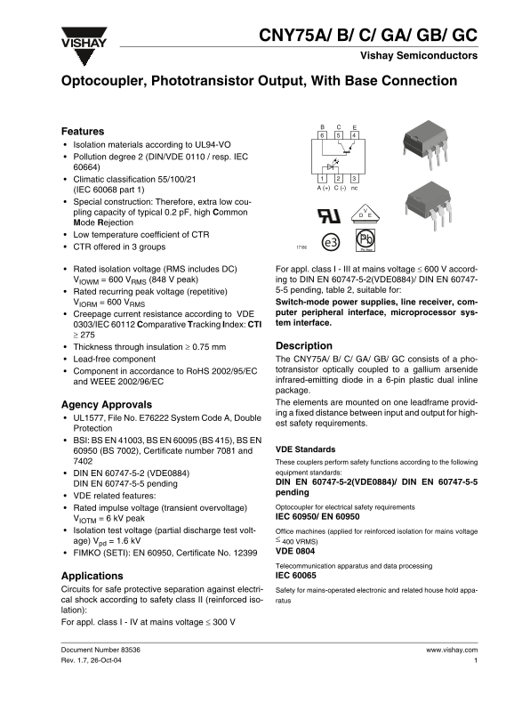
Page 1 Text Content
CNY75A/ B/ C/ GA/ GB/ GC
Vishay Semiconductors
Optocoupler, Phototransistor Output, With Base Connection
Features Isolation materials according to UL94-VO Pollution degree 2 (DIN/VDE 0110 / resp. IEC 60664) Climatic classification 55/100/21
(-)A nc C
(IEC 60068 part 1) Special construction: Therefore, extra low cou- pling capacity of typical 0.2 p F, high Common Mode Rejection Low temperature coefficient of CTR
e3 Pb
CTR offered in 3 groups Pb-free
Rated isolation voltage (RMS includes DC) For appl. class I - III at mains voltage ≤ 600 V accord- VIOWM = 600 VRMS (848 V peak) ing to DIN EN 60747-5-2(VDE0884)/ DIN EN 60747-
Rated recurring peak voltage (repetitive) 5-5 pending, table 2, suitable for: VIORM = 600 VRMS Switch-mode power supplies, line receiver, com- Creepage current resistance according to VDE puter peripheral interface, microprocessor sys- 0303/IEC 60112 Comparative Tracking Index: CTI tem interface.
Thickness through insulation ≥ 0.75 mm Description
Lead-free component The CNY75A/ B/ C/ GA/ GB/ GC consists of a pho-
Component in accordance to Ro HS 2002/95/EC totransistor optically coupled to a gallium arsenide and WEEE 2002/96/EC infrared-emitting diode in a 6-pin plastic dual inline package. The elements are mounted on one leadframe provid-
Agency Approvals
ing a fixed distance between input and output for high-
UL1577, File No. E76222 System Code A, Double
est safety requirements.
Protection BSI: BS EN 41003, BS EN 60095 (BS 415), BS EN
60950 (BS 7002), Certificate number 7081 and VDE Standards These couplers perform safety functions according to the following DIN EN 60747-5-2 (VDE0884) equipment standards: DIN EN 60747-5-5 pending DIN EN 60747-5-2(VDE0884)/ DIN EN 60747-5-5 pending
VDE related features:
Rated impulse voltage (transient overvoltage) Optocoupler for electrical safety requirements VIOTM = 6 k V peak IEC 60950/ EN 60950
Isolation test voltage (partial discharge test volt- Office machines (applied for reinforced isolation for mains voltage
age) Vpd = 1.6 k V ≤ 400 VRMS) FIMKO (SETI): EN 60950, Certificate No. 12399 VDE 0804 Telecommunication apparatus and data processing Applications IEC 60065
Circuits for safe protective separation against electri- Safety for mains-operated electronic and related house hold appa- cal shock according to safety class II (reinforced iso- ratus lation): For appl. class I - IV at mains voltage ≤ 300 V
Document Number 83536 www.vishay.com Rev. 1.7, 26-Oct-04
Page Summary Contents For VISHAY CNY75A B C GA GB GC Optocoupler, Phototransistor Output, With Base Connection
Manual Details
| Brand | Vishay |
|---|---|
| Pages | 11 |
| File Size | 212.23 KB |
| Published | May 31, 2026 |
Enter the captcha to get the download link:
