Toshiba TOSHIBA 2SK2615 User's Manual
Summary
Explore the high performance of this N Channel MOS Field Effect Transistor (MOSFET), ideal for demanding power control applications such as DC-DC conversion, relay driving, and motor control circuits. This technical manual provides comprehensive documentation for engineers, detailing absolute maximum ratings, detailed electrical characteristics, thermal parameters, and switching time analysis. Designed for a wide range of general electronic equipment—including industrial robotics, computing, and consumer appliances—it ensures proper system design while adhering to best practices for handling highly sensitive semiconductor devices.
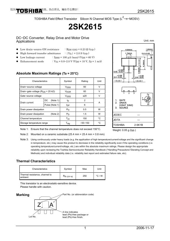
Page 1 Text Content
2SK2615
TOSHIBA Field Effect Transistor Silicon N Channel MOS Type (L2−π−MOSV)
2SK2615
DC−DC Converter, Relay Drive and Motor Drive
Unit: mm
Applications
Low drain−source ON resistance : RDS (ON) = 0.23 Ω (typ.) High forward transfer admittance : |Yfs| = 2.0 S (typ.) Low leakage current : IDSS = 100 μA (max) (VDS = 60 V) Enhancement mode : Vth = 0.8~2.0 V (VDS = 10 V, ID = 1 m A)
Absolute Maximum Ratings (Ta = 25°C)
Characteristics Symbol Rating Unit
Drain−source voltage VDSS 60 V
Drain−gate voltage (RGS = 20 kΩ) VDGR 60 V
Gate−source voltage VGSS ±20 V
DC (Note 1) ID 2
Drain current
Pulse (Note 1) IDP 6
Drain power dissipation PD 0.5 W
Drain power dissipation (Note 2) PD 1.5 W
JEDEC ―
Channel temperature Tch 150 °C
JEITA ―
Storage temperature range Tstg −55~150 °C
TOSHIBA 2-5K1B
Note 1: Ensure that the channel temperature does not exceed 150°C.
Weight: 0.05 g (typ.)
Note 2: Mounted on a ceramic substrate (25.4 mm × 25.4 mm × 0.8 mm)
Note 3: Using continuously under heavy loads (e.g. the application of high temperature/current/voltage and the significant change
in temperature, etc.) may cause this product to decrease in the reliability significantly even if the operating conditions (i.e. operating temperature/current/voltage, etc.) are within the absolute maximum ratings. Please design the appropriate reliability upon reviewing the Toshiba Semiconductor Reliability Handbook (“Handling Precautions”/Derating Concept and Methods) and individual reliability data (i.e. reliability test report and estimated failure rate, etc).
Thermal Characteristics
Characteristics Symbol Max Unit
Thermal resistance, channel to ambient Rth (ch−a) 250 °C / W
This transistor is an electrostatic-sensitive device. Please handle with caution.
Marking Part No. (or abbreviation code)
A line indicates lead (Pb)-free package or
Lot No. lead (Pb)-free finish.
Page Summary Contents For Toshiba TOSHIBA 2SK2615 User's Manual
Manual Details
| Brand | Toshiba |
|---|---|
| Pages | 6 |
| File Size | 659.32 KB |
| Published | June 02, 2026 |
Enter the captcha to get the download link:

Frequently Asked Questions
What critical precaution is required for reliable usage under heavy loads?
Designers must consult the Reliability Handbook for appropriate derating concepts and methods.