Toshiba TB6612FNG User Guide (1)
Summary
The TB6612FNG is a reliable driver IC designed for controlling dual DC motors in various electronic applications, providing robust performance up to 3.2A peak output current. This module supports multiple operational modes including Clockwise (CW), Counter-Clockwise (CCW), short brake, and stop functions via simple control inputs. The comprehensive manual details the device's detailed pin configuration, electrical characteristics, low ON-resistance functionality, power saving modes, and necessary handling precautions for easy integration by hardware engineers and electronics hobbyists.
Page 1 Text Content
TB6612FNG
Toshiba Bi-CD Integrated Circuit Silicon Monolithic
TB6612FNG
Driver IC for Dual DC motor
TB6612FNG is a driver IC for DC motor with output transistor in LD MOS structure with low ON-resistor. Two input signals, IN1 and IN2, can choose one of four modes such as CW, CCW, short brake, and stop mode.
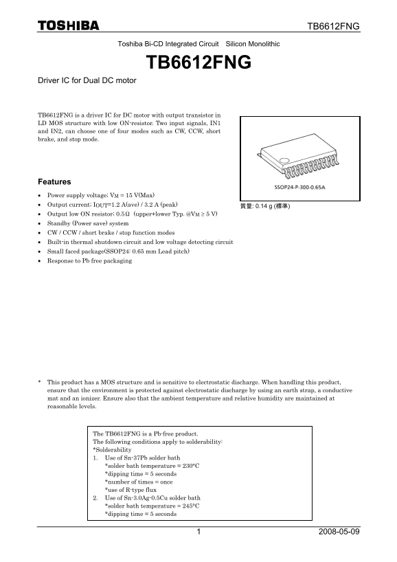
Features • Power supply voltage; VM = 15 V(Max) • Output current; IOUT=1.2 A(ave) / 3.2 A (peak) 質量: 0.14 g (標準) • Output low ON resistor; 0.5Ω (upper+lower Typ. @VM ≥ 5 V) • Standby (Power save) system • CW / CCW / short brake / stop function modes • Built-in thermal shutdown circuit and low voltage detecting circuit • Small faced package(SSOP24: 0.65 mm Lead pitch) • Response to Pb free packaging
* This product has a MOS structure and is sensitive to electrostatic discharge. When handling this product, ensure that the environment is protected against electrostatic discharge by using an earth strap, a conductive mat and an ionizer. Ensure also that the ambient temperature and relative humidity are maintained at reasonable levels.
The TB6612FNG is a Pb-free product. The following conditions apply to solderability: *Solderability 1. Use of Sn-37Pb solder bath *solder bath temperature = 230°C *dipping time = 5 seconds *number of times = once *use of R-type flux 2. Use of Sn-3.0Ag-0.5Cu solder bath *solder bath temperature = 245°C *dipping time = 5 seconds
Page Summary Contents For Toshiba TB6612FNG User Guide (1)
Manual Details
| Brand | Toshiba |
|---|---|
| Pages | 11 |
| File Size | 300.88 KB |
| Published | June 15, 2026 |
Enter the captcha to get the download link:

Frequently Asked Questions
What modes can the TB6612FNG operate?
It supports CW, CCW, short brake, and stop functions via two input signals (IN1 and IN2).
What is the maximum output current capability of the device?
The device offers 1.2 A average and 3.2 A peak output current.
How must the product be handled due to its structure?
Since it has a MOS structure, handling requires protection from electrostatic discharge (ESD) using an earth strap and conductive mat.
What solderability conditions apply if using Sn-37Pb solder bath?
The temperature should be 230°C for 5 seconds, used once with R-type flux.