Toshiba TOSHIBA 2SK2613 Owner's Manual (1), (1) User Guide
Summary
This technical datasheet details the 2SK2613 MOSFET, a high-performance N Channel device engineered for demanding power switching roles, including DC-DC converters and motor drive applications. The manual provides comprehensive electrical characteristics, absolute maximum ratings, thermal analysis, and detailed I-V curves crucial for reliable circuit design. It is an essential resource for professional electrical engineers developing general commercial electronics such as industrial controls, appliances, and computing equipment.
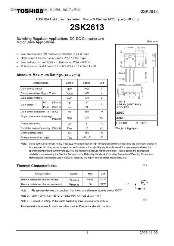
Page 1 Text Content
2SK2613
TOSHIBA Field Effect Transistor Silicon N Channel MOS Type (π-MOSIII)
2SK2613
Switching Regulator Applications, DC-DC Converter and
Unit: mm
Motor Drive Applications
• Low drain-source ON resistance: RDS (ON) = 1.4 Ω (typ.) • High forward transfer admittance: ⎪Yfs⎪ = 6.0 S (typ.) • Low leakage current: IDSS = 100 μA (max) (VDS = 800 V) • Enhancement-model: Vth = 2.0~4.0 V (VDS = 10 V, ID = 1 m A)
Absolute Maximum Ratings (Ta = 25°C)
Characteristics Symbol Rating Unit
Drain-source voltage VDSS 1000 V
Drain-gate voltage (RGS = 20 kΩ) VDGR 1000 V
Gate-source voltage VGSS ±30 V
1. GATE
DC (Note 1) ID 8
Drain current 2. DRAIN (HEAT SINK)
Pulse (Note 1) IDP 24 3. SOURSE
Drain power dissipation (Tc = 25°C) PD 150 W
JEDEC ―
Single pulse avalanche energy
JEITA ―
(Note 2) EAS 910 m J
Avalanche current IAR 8 A TOSHIBA 2−16C1B
Repetitive avalanche energy (Note 3) EAR 15 m J Weight: 4.6 g (typ.) Channel temperature Tch 150 °C
Storage temperature range Tstg −55~150 °C
Note: Using continuously under heavy loads (e.g. the application of high temperature/current/voltage and the significant change in temperature, etc.) may cause this product to decrease in the reliability significantly even if the operating conditions (i.e. operating temperature/current/voltage, etc.) are within the absolute maximum ratings. Please design the appropriate reliability upon reviewing the Toshiba Semiconductor Reliability Handbook (“Handling Precautions”/Derating Concept and Methods) and individual reliability data (i.e. reliability test report and estimated failure rate, etc).
Thermal Characteristics
Characteristics Symbol Max Unit
Thermal resistance, channel to case Rth (ch-c) 0.833 °C/W
Thermal resistance, channel to ambient Rth (ch-a) 50 °C/W
Note 1: Please use devices on condition that the channel temperature is below 150°C.
Note 2: VDD = 90 V, Tch = 25°C, L = 26.3 m H, RG = 25 Ω, IAR = 8 A
Note 3: Repetitive rating: Pulse width limited by max junction temperature
This transistor is an electrostatic sensitive device. Please handle with caution.
Page Summary Contents For Toshiba TOSHIBA 2SK2613 Owner's Manual (1), (1) User Guide
Manual Details
| Brand | Toshiba |
|---|---|
| Pages | 6 |
| File Size | 221.66 KB |
| Published | June 02, 2026 |
Enter the captcha to get the download link:

Frequently Asked Questions
What is the maximum rated drain-source voltage (V_DSS)?
The absolute maximum rating for the drain-source voltage is 1000 V.
What precautions must be taken when handling this component?
Because it is an electrostatic sensitive device, please handle with extreme caution.
How do I ensure reliable operation under heavy load or temperature changes?
You must review the Toshiba Reliability Handbook and apply proper derating concepts for stable design.
Can this product be used in critical life-safety systems (e.g., medical devices)?
No, it is not warranted for use in equipment where failure could cause loss of human life or bodily injury.