# A B C D E F G H I J K L M N O P Q R S T U V W X Y Z

Texas Instruments TPS61020, TPS61024 TPS61025, TPS61027, TPS61028 Data Sheet

Summary

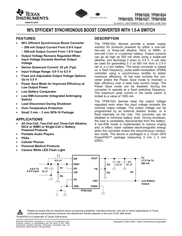
This high-efficiency synchronous boost converter series provides stable, regulated power conversion for a wide range of low-power portable electronics. Capable of managing multiple battery types—including single-cell Li-Ion and alkaline chemistry—it guarantees performance even with extreme input voltage fluctuations. With high efficiency (up to 96%) and integrated protective features, the product is essential for engineers designing PDAs, medical devices, audio players, cellular phones, and portable cameras requiring reliable, compact energy management solutions.
📄 Preview 📖 Table of Contents Contents PAGE OF 26

Page 1 Text Content

TPS61020, TPS61024

(3,25 mm x 3,25 mm)

TPS61025, TPS61027, TPS61028

www.ti.com

SLVS451C–SEPTEMBER 2003–REVISED JUNE

96% EFFICIENT SYNCHRONOUS BOOST CONVERTER WITH 1.5-A SWITCH

FEATURES DESCRIPTION

96% Efficient Synchronous Boost Converter

The TPS6102x devices provide power supply

200-m A Output Current From 0.9-V Input solution for products powered by either one-cell,–

two-cell, or three-cell alkaline, Ni Cd or Ni MH, or–

500-m A Output Current From 1.8-V Input

one-cell Li-Ion or Li-polymer battery. Output currents

Output Voltage Remains Regulated When

can go as high as m A while using single-cell

Input Voltage Exceeds Nominal Output

alkaline, and discharge it down to 0.9 V. It can also

Voltage be used for generating at m A from 3.3-V

rail or Li-Ion battery. The boost converter is based•

Device Quiescent Current: µA (Typ)

on fixed frequency, pulse-width-modulation (PWM)•

Input Voltage Range: 0.9 to 6.5

controller using synchronous rectifier to obtain

Fixed and Adjustable Output Voltage Options

maximum efficiency. At low load currents the con-

Up to 5.5 verter enters the Power Save mode to maintain

high efficiency over wide load current range. The•

Power Save Mode for Improved Efficiency at

Power Save mode can be disabled, forcing the Low

Output Power

converter to operate at fixed switching frequency.

Low Battery Comparator

The maximum peak current in the boost switch is

Low EMI-Converter (Integrated Antiringing limited to value of m A.

Switch)

The TPS6102x devices keep the output voltage

Load Disconnect During Shutdown

regulated even when the input voltage exceeds the

Over-Temperature Protection nominal output voltage. The output voltage can be•

programmed by an external resistor divider, or is•

Small mm mm QFN-10 Package

fixed internally on the chip. The converter can be

disabled to minimize battery drain. During shutdown,

APPLICATIONS

the load is completely disconnected from the battery.

All One-Cell, Two-Cell and Three-Cell Alkaline,

low-EMI mode is implemented to reduce ringing

Ni Cd or Ni MH or Single-Cell Li Battery

and, in effect, lower radiated electromagnetic energy

Powered Products

when the converter enters the discontinuous conduc-

Portable Audio Players tion mode. The device is packaged in 10-pin QFN

Power PAD™ package measuring mm mm•

(DRC).•

Cellular Phones

Personal Medical Products

Camera White LED Flash Light

SW VOUT

6.8 µH 3.3 V Up To

VBAT R3 2.2 µF 47 µF

C1 R1 EN

0.9-V To FB 6.5-V Input 10 µF

LBI R4 R5

LBO Low Battery

Output

GND PGND TPS61020

Please be aware that an important notice concerning availability, standard warranty, and use in critical applications of Texas

Instruments semiconductor products and disclaimers thereto appears at the end of this data sheet.

Power PAD is trademark of Texas Instruments.

PRODUCTION DATA information is current as of publication date. Copyright 2003–2005, Texas Instruments Incorporated

Products conform to specifications per the terms of the Texas

Instruments standard warranty. Production processing does not

necessarily include testing of all parameters.

Page Summary Contents For Texas Instruments TPS61020, TPS61024 TPS61025, TPS61027, TPS61028 Data Sheet

Page 1 TPS61020, TPS61024 (3,25 mm x 3,25 mm) TPS61025, TPS61027, TPS61028 www.ti.com SLVS451C–SEPTEMBER 2003–REVISED JUNE 96% EFFICIENT SYNCHRONOUS BOOST CONVERTER WITH 1.5-A SWITCH FEATURES DESCRIPTION 96%...
Page 2 TPS61020, TPS61024 TPS61025, TPS61027, TPS61028 www.ti.com SLVS451C–SEPTEMBER 2003–REVISED JUNE These devices have limited built-in ESD protection. The leads should be shorted together or the device p...
Page 3 TPS61020, TPS61024 TPS61025, TPS61027, TPS61028 www.ti.com SLVS451C–SEPTEMBER 2003–REVISED JUNE ELECTRICAL CHARACTERISTICS over recommended free-air temperature range and over recommended input voltag...
Page 4 TPS61020, TPS61024 TPS61025, TPS61027, TPS61028 www.ti.com SLVS451C–SEPTEMBER 2003–REVISED JUNE PIN ASSIGNMENTS DRC PACKAGE (TOP VIEW) EN PGND SWVOUT FB PS LBO LBI GND VBAT Terminal Functions TERMINAL...
Page 5 TPS61020, TPS61024 TPS61025, TPS61027, TPS61028 www.ti.com SLVS451C–SEPTEMBER 2003–REVISED JUNE FUNCTIONAL BLOCK DIAGRAM (TPS61020, TPS61028) Backgate Control Anti- Ringing VOUT Vmax Gate Control Cont...
Page 6 TPS61020, TPS61024 TPS61025, TPS61027, TPS61028 www.ti.com SLVS451C–SEPTEMBER 2003–REVISED JUNE PARAMETER MEASUREMENT INFORMATION SW VOUT VCC C2 C3 Boost Output VBAT R3 2.2 µF 47 µF Power C1 R1 EN Sup...
Page 7 TPS61020, TPS61024 TPS61025, TPS61027, TPS61028 www.ti.com SLVS451C–SEPTEMBER 2003–REVISED JUNE ff ic ie cy ax im tp t C rr en t - MAXIMUM OUTPUT CURRENT TPS61020 vs EFFICIENCY INPUT VOLTAGE vs OUTPUT...
Page 8 TPS61020, TPS61024 TPS61025, TPS61027, TPS61028 www.ti.com SLVS451C–SEPTEMBER 2003–REVISED JUNE tp lta - V ff ic ie cy TPS61025 TPS61027 EFFICIENCY EFFICIENCY vs vs INPUT VOLTAGE INPUT VOLTAGE VO = 3....
Page 9 TPS61020, TPS61024 TPS61025, TPS61027, TPS61028 www.ti.com SLVS451C–SEPTEMBER 2003–REVISED JUNE ad ly rr en t I to In ct rr en tp lt ag /d iv /d iv NO LOAD SUPPLY CURRENT INTO VBAT NO LOAD SUPPLY CURR...
Page 10 TPS61020, TPS61024 TPS61025, TPS61027, TPS61028 www.ti.com SLVS451C–SEPTEMBER 2003–REVISED JUNE In ct rr en tp lt ag tp lt ag tp rr en /d iv , D /d iv , A TPS61025 /d iv , A /d iv , D TPS61027 OUTPUT ...
Page 11 TPS61020, TPS61024 TPS61025, TPS61027, TPS61028 www.ti.com tp lt ag SLVS451C–SEPTEMBER ab le 2003–REVISED JUNE /d iv , D /d iv , D tp lt ag In t V lt ag /d iv , A /d iv , A TPS61025 TPS61027 LINE TRAN...
Page 12 TPS61020, TPS61024 TPS61025, TPS61027, TPS61028 www.ti.com SLVS451C–SEPTEMBER 2003–REVISED JUNE DETAILED DESCRIPTION CONTROLLER CIRCUIT The controller circuit of the device is based on fixed frequency...
Page 13 TPS61020, TPS61024 TPS61025, TPS61027, TPS61028 www.ti.com SLVS451C–SEPTEMBER 2003–REVISED JUNE DETAILED DESCRIPTION (continued) Undervoltage Lockout An undervoltage lockout function prevents device s...
Page 14 TPS61020, TPS61024 TPS61025, TPS61027, TPS61028 www.ti.com SLVS451C–SEPTEMBER 2003–REVISED JUNE DETAILED DESCRIPTION (continued) Low Battery Detector Circuit—LBI/LBO The low-battery detector circuit i...
Page 15 TPS61020, TPS61024 TPS61025, TPS61027, TPS61028 www.ti.com SLVS451C–SEPTEMBER 2003–REVISED JUNE APPLICATION INFORMATION DESIGN PROCEDURE The TPS6102x dc/dc converters are intended for systems powered ...
Page 16 TPS61020, TPS61024 TPS61025, TPS61027, TPS61028 www.ti.com SLVS451C–SEPTEMBER 2003–REVISED JUNE VBAT VBAT VLBIthreshold m V The output of the low battery supervisor is simple open-drain output that g...
Page 17 TPS61020, TPS61024 TPS61025, TPS61027, TPS61028 www.ti.com SLVS451C–SEPTEMBER 2003–REVISED JUNE Capacitor Selection Input Capacitor At least 10-µF input capacitor is recommended to improve transient b...
Page 18 TPS61020, TPS61024 TPS61025, TPS61027, TPS61028 www.ti.com SLVS451C–SEPTEMBER 2003–REVISED JUNE APPLICATION EXAMPLES VCC 5 V SW VOUT 6.8 µH Boost Output Battery VBAT 2.2 µF 100 µF Input C1 R1 EN LBI R...
Page 19 TPS61020, TPS61024 TPS61025, TPS61027, TPS61028 www.ti.com SLVS451C–SEPTEMBER 2003–REVISED JUNE TPS61020 SW VOUT Input C1 0.9 V to 6.5 V LBI FB PS R1 GND PGND List of Components: U1 = TPS61020DRC L1 =...
Page 20 TPS61020, TPS61024 TPS61025, TPS61027, TPS61028 www.ti.com SLVS451C–SEPTEMBER 2003–REVISED JUNE VCC2 10 V C5 Unregulated Auxiliary Output SW VCC1 5 V Boost Main Output Battery VBAT 2.2 µF 47 µF Input ...
Page 21 TPS61020, TPS61024 TPS61025, TPS61027, TPS61028 www.ti.com SLVS451C–SEPTEMBER 2003–REVISED JUNE THERMAL INFORMATION Implementation of integrated circuits in low-profile and fine-pitch surface-mount pa...
Page 24 PACKAGE OPTION ADDENDUM www.ti.com 8-Aug-2005 PACKAGING INFORMATION Orderable Device Status Package Package Pins Package Eco Plan Lead/Ball Finish MSL Peak Temp Type Drawing Qty TPS61020DRCR ACTIVE SO...
Page 26 IMPORTANT NOTICE Texas Instruments Incorporated and its subsidiaries (TI) reserve the right to make corrections, modifications, enhancements, improvements, and other changes to its products and servic...

Manual Details

Brand Texas Instruments
Pages 26
File Size 953.27 KB
Published June 05, 2026
56 views

Enter the captcha to get the download link:

captcha

Frequently Asked Questions

What is the acceptable input voltage range for this converter?

The device operates efficiently with an input voltage range of 0.9 V to 6.5 V.

How does it maintain efficiency at low power usage?

It enters a Power Save mode, which can be controlled or disabled depending on the application needs.

What safety features protect against battery depletion during shutdown?

The device includes a Low Battery Comparator and ensures the output voltage remains regulated even upon shutdown.

How should I safely store or handle the component to avoid damage?

Because it has limited built-in ESD protection, leads must be shorted together or placed in conductive foam for storage.