Texas Instruments TPS1100, TPS1100Y Data Sheet
Summary
Design efficient, low-voltage circuits with the TPS1100 MOSFET, an optimized single P-channel enhancement-mode device ideal for portable battery management systems running on 3V or 5V power. This manual provides comprehensive documentation covering electrical characteristics, advanced packaging options (including ultrathin TSSOP), and robust features like up to 2kV ESD protection. Perfect for engineers developing notebook computers, PDAs, or motor drivers where maximizing battery life and minimizing board space is critical.
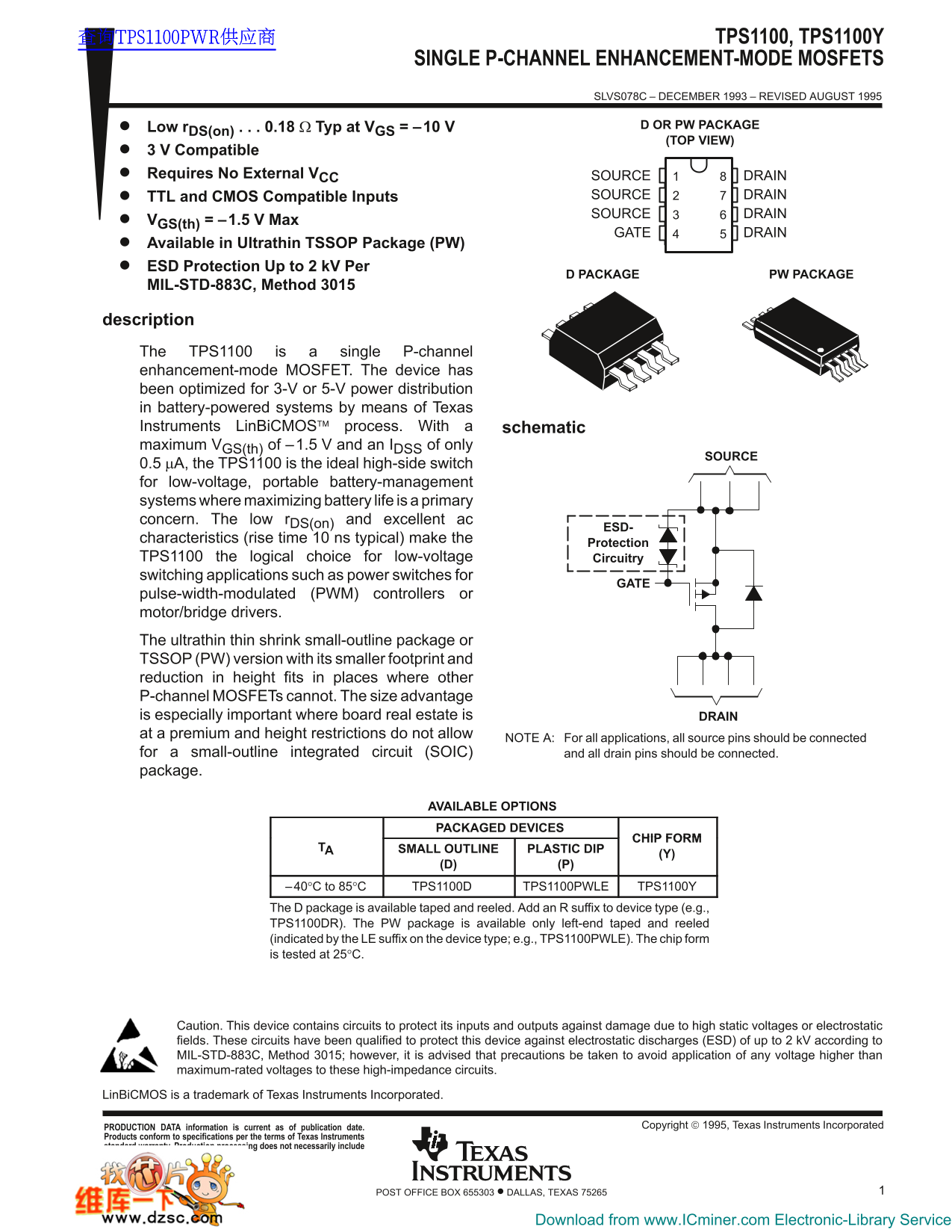
Page 1 Text Content
查询TPS1100PWR供应商 TPS1100, TPS1100Y
SINGLE P-CHANNEL ENHANCEMENT-MODE MOSFETS
SLVS078C – DECEMBER 1993 – REVISED AUGUST 1995
Low r DS(on) 0.18 Ω Typ at VGS = –10 V D OR PW PACKAGE (TOP VIEW)
3 V Compatible Requires No External VCC SOURCE DRAIN
TTL and CMOS Compatible Inputs SOURCE DRAIN SOURCE DRAIN
VGS(th) = –1.5 V Max
GATE DRAIN
Available in Ultrathin TSSOP Package (PW) ESD Protection Up to 2 k V Per
D PACKAGE PW PACKAGE
MIL-STD-883C, Method 3015
description The TPS1100 is a single P-channel enhancement-mode MOSFET. The device has been optimized for 3-V or 5-V power distribution in battery-powered systems by means of Texas Instruments Lin Bi CMOS process. With a schematic maximum VGS(th) of –1.5 V and an IDSS of only
SOURCE
0.5 µA, the TPS1100 is the ideal high-side switch for low-voltage, portable battery-management systems where maximizing battery life is a primary concern. The low r DS(on) and excellent ac
characteristics (rise time 10 ns typical) make the
Protection
TPS1100 the logical choice for low-voltage Circuitry switching applications such as power switches for
pulse-width-modulated (PWM) controllers or motor/bridge drivers. The ultrathin thin shrink small-outline package or TSSOP (PW) version with its smaller footprint and reduction in height fits in places where other P-channel MOSFETs cannot. The size advantage is especially important where board real estate is DRAIN at a premium and height restrictions do not allow
NOTE A: For all applications, all source pins should be connected
for a small-outline integrated circuit (SOIC) and all drain pins should be connected. package.
AVAILABLE OPTIONS PACKAGED DEVICES
CHIP FORM
TA SMALL OUTLINE PLASTIC DIP
–40°C to 85°C TPS1100D TPS1100PWLE TPS1100Y The D package is available taped and reeled. Add an R suffix to device type (e.g., TPS1100DR). The PW package is available only left-end taped and reeled (indicated by the LE suffix on the device type; e.g., TPS1100PWLE). The chip form is tested at 25°C.
Caution. This device contains circuits to protect its inputs and outputs against damage due to high static voltages or electrostatic fields. These circuits have been qualified to protect this device against electrostatic discharges (ESD) of up to 2 k V according to MIL-STD-883C, Method 3015; however, it is advised that precautions be taken to avoid application of any voltage higher than maximum-rated voltages to these high-impedance circuits.
Lin Bi CMOS is a trademark of Texas Instruments Incorporated.
Copyright 1995, Texas Instruments Incorporated PRODUCTION DATA information is current as of publication date.
Products conform to specifications per the terms of Texas Instruments standard warranty. Production processing does not necessarily include testing of all parameters.
1POST OFFICE BOX 655303 • DALLAS, TEXAS 75265
Download from www.ICminer.com Electronic-Library Service
Page Summary Contents For Texas Instruments TPS1100, TPS1100Y Data Sheet
Manual Details
| Brand | Texas Instruments |
|---|---|
| Pages | 10 |
| File Size | 191.18 KB |
| Published | July 22, 2026 |
Enter the captcha to get the download link:

Frequently Asked Questions
What makes the TPS1100 suitable for battery-powered systems?
It is optimized for 3-V or 5-V power distribution, making it an ideal high-side switch where maximizing battery life is crucial.
Does this device offer protection against static discharge?
Yes, the device features ESD Protection up to 2 kV per package according to MIL-STD-883C, Method 3015.
Which packaging option minimizes board space usage?
The Ultrathin TSSOP (PW) version offers a smaller footprint and reduced height compared to other options.
What are some recommended applications for the TPS1100 MOSFET?
It is designed for low-voltage circuitry switching in devices like notebook computers, PDAs, cellular telephones, and PCMCIA cards.