Texas Instruments TLV27L1 TLV27L2 Data Sheet Manual
Summary
Discover the TLV27Lx series, a family of ultra-low power operational amplifiers featuring robust rail-to-rail output capability and high bandwidth performance (160 kHz). Ideal for designers creating portable medical equipment, low-power security detection systems, and instrumentation requiring stable operation. This comprehensive manual provides detailed technical specifications, selection guides, and ordering information for models designed for both commercial and industrial temperature ranges, ensuring optimal power efficiency in demanding applications.
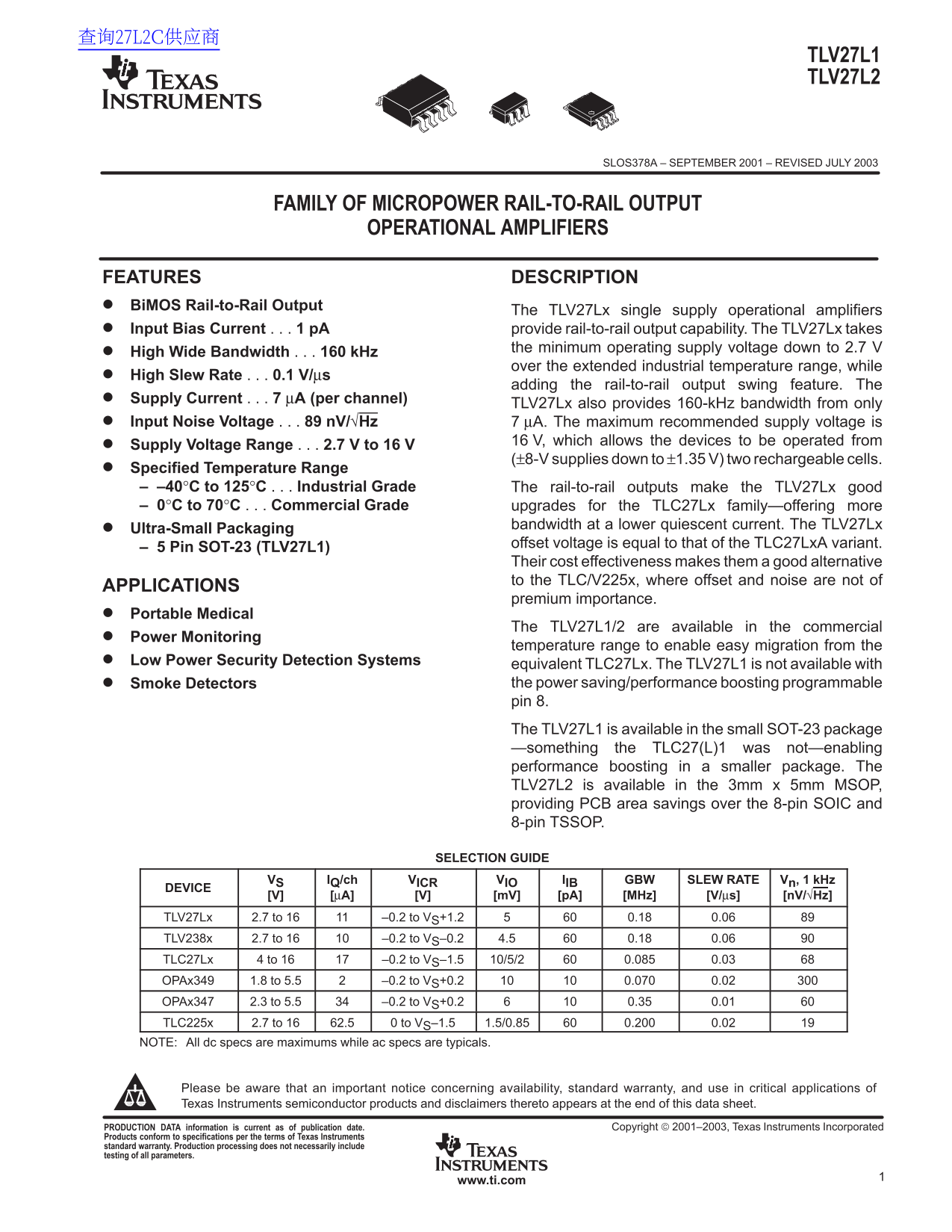
Page 1 Text Content
TLV27L1 TLV27L2
SLOS378A – SEPTEMBER 2001 – REVISED JULY 2003
FAMILY OF MICROPOWER RAIL-TO-RAIL OUTPUT
OPERATIONAL AMPLIFIERS
FEATURES DESCRIPTION Bi MOS Rail-to-Rail Output
The TLV27Lx single supply operational amplifiers
Input Bias Current 1 p A provide rail-to-rail output capability. The TLV27Lx takes
the minimum operating supply voltage down to 2.7 V
High Wide Bandwidth 160 k Hz
over the extended industrial temperature range, while
High Slew Rate 0.1 V/µs
adding the rail-to-rail output swing feature. The
Supply Current 7 µA (per channel)
TLV27Lx also provides 160-k Hz bandwidth from only
Input Noise Voltage 89 n V/√Hz µA. The maximum recommended supply voltage is
V, which allows the devices to be operated from
Supply Voltage Range 2.7 V to 16 V
(±8-V supplies down to ±1.35 V) two rechargeable cells.
Specified Temperature Range – –40°C to 125°C Industrial Grade The rail-to-rail outputs make the TLV27Lx good – 0°C to 70°C Commercial Grade upgrades for the TLC27Lx family—offering more
bandwidth at a lower quiescent current. The TLV27Lx
Ultra-Small Packaging
offset voltage is equal to that of the TLC27Lx A variant.
– 5 Pin SOT-23 (TLV27L1)
Their cost effectiveness makes them a good alternative to the TLC/V225x, where offset and noise are not of
APPLICATIONS
premium importance.
Portable Medical
The TLV27L1/2 are available in the commercial
Power Monitoring
temperature range to enable easy migration from the
Low Power Security Detection Systems equivalent TLC27Lx. The TLV27L1 is not available with
Smoke Detectors the power saving/performance boosting programmable pin 8. The TLV27L1 is available in the small SOT-23 package —something the TLC27(L)1 was not—enabling performance boosting in a smaller package. The TLV27L2 is available in the 3mm x 5mm MSOP, providing PCB area savings over the 8-pin SOIC and 8-pin TSSOP.
SELECTION GUIDE
VS IQ/ch VICR VIO IIB GBW SLEW RATE Vn, 1 k Hz
DEVICE
[V] [µA] [V] [m V] [p A] [MHz] [V/µs] [n V/√Hz]
TLV27Lx 2.7 to 16 –0.2 to VS+1.2 0.18 0.06 TLV238x 2.7 to 16 –0.2 to VS–0.2 4.5 0.18 0.06 TLC27Lx 4 to 16 –0.2 to VS–1.5 10/5/2 0.085 0.03 OPAx349 1.8 to 5.5 –0.2 to VS+0.2 0.070 0.02 OPAx347 2.3 to 5.5 –0.2 to VS+0.2 0.35 0.01 TLC225x 2.7 to 16 62.5 0 to VS–1.5 1.5/0.85 0.200 0.02 NOTE: All dc specs are maximums while ac specs are typicals.
Please be aware that an important notice concerning availability, standard warranty, and use in critical applications of Texas Instruments semiconductor products and disclaimers thereto appears at the end of this data sheet.
PRODUCTION DATA information is current as of publication date. Copyright 2001–2003, Texas Instruments Incorporated
Products conform to specifications per the terms of Texas Instruments standard warranty. Production processing does not necessarily include testing of all parameters.
1www.ti.com
Page Summary Contents For Texas Instruments TLV27L1 TLV27L2 Data Sheet Manual
Manual Details
| Brand | Texas Instruments |
|---|---|
| Pages | 12 |
| File Size | 261.75 KB |
| Published | July 16, 2026 |
Enter the captcha to get the download link:

Frequently Asked Questions
What is the operating temperature range for different versions?
The TLV27L1I/TLV27L2I variants support an Industrial Grade range of -40°C to 125°C, while non-I variants are rated for a Commercial Grade range of 0°C to 70°C.
What is the voltage supply required for these amplifiers?
The TLV27Lx family can operate from a minimum of 2.7 V up to a maximum of 16 V, or provide dual supplies down to ±1.35 V on ±8-V supplies.
Which package options are available for the devices?
Devices come in multiple packages, including the small SOT-23 (TLV27L1), MSOP (TLV27L2), SOIC-8, and TSSOP types to save PCB area.
How does this device perform regarding power efficiency?
It is noted for its low supply current of 7 µA per channel and offers options like the TLV27L1, which focuses on cost effectiveness and low power consumption.