# A B C D E F G H I J K L M N O P Q R S T U V W X Y Z

Texas Instruments THS1041 Data Sheet / Manual

Summary

Discover the THS1041, a highly versatile 10-bit, 40 MSPS Analog-to-Digital Converter optimized for imaging and video applications. Featuring built-in programmable gain amplification (PGA) and advanced clamping functions, this low-power ADC adapts to single-supply operation and provides robust signal integrity. The manual details the device’s architecture, I/O specifications, operational modes, and temperature grades. It is ideally suited for developers working on set-top boxes, video surveillance, color scanners, digital copiers, and advanced communication systems.
📄 Preview PAGE OF 37

Page 1 Text Content

查询THS1041供应商

THS1041

SLAS289B – OCTOBER 2001 – REVISED FEBRUARY 2002

10-Bit, 40-MSPS ANALOG-TO-DIGITAL CONVERTER

WITH PGA AND CLAMP

FEATURES references to match the user’s design requirements. For more design flexibility, the internal reference can be

Analog Supply 3 V

bypassed to use an external reference to suit the dc

Digital Supply 3 V accuracy and temperature drift requirements of the

Configurable Input Functions: application. The out-of-range output indicates any – Single-Ended out-of-range condition in THS1041’s input signal. The – Single-Ended With Analog Clamp format of the digital output can be coded in either – Single-Ended With Programmable Digital unsigned binary or 2s complement.

Clamp

The speed, resolution, and single-supply operation of

– Differential

the THS1041 are suited to applications in set-top-box

Built-In Programmable Gain Amplifier (PGA) (STB), video, multimedia, imaging, high-speed

Differential Nonlinearity: ±0.45 LSB acquisition, and communications. The built-in clamp function allows dc restoration of a video signal and is

Signal-to-Noise: 60 d B Typ at 4.8 MHz

suitable for video applications. The speed and

Spurious Free Dynamic Range: 72 d B

resolution ideally suit charge-couple device (CCD) input

Adjustable Internal Voltage Reference systems such as color scanners, digital copiers, digital

Unsigned Binary/2s Complement Output cameras, and camcorders. A wide input voltage range allows the THS1041 to be applied in both imaging and

Out-of-Range Indicator

communications systems.

Power-Down Mode

The THS1041C is characterized for operation from 0°C APPLICATIONS to 70°C, while the THS1041I is characterized for operation from –40°C to 85°C.

Video/CCD Imaging

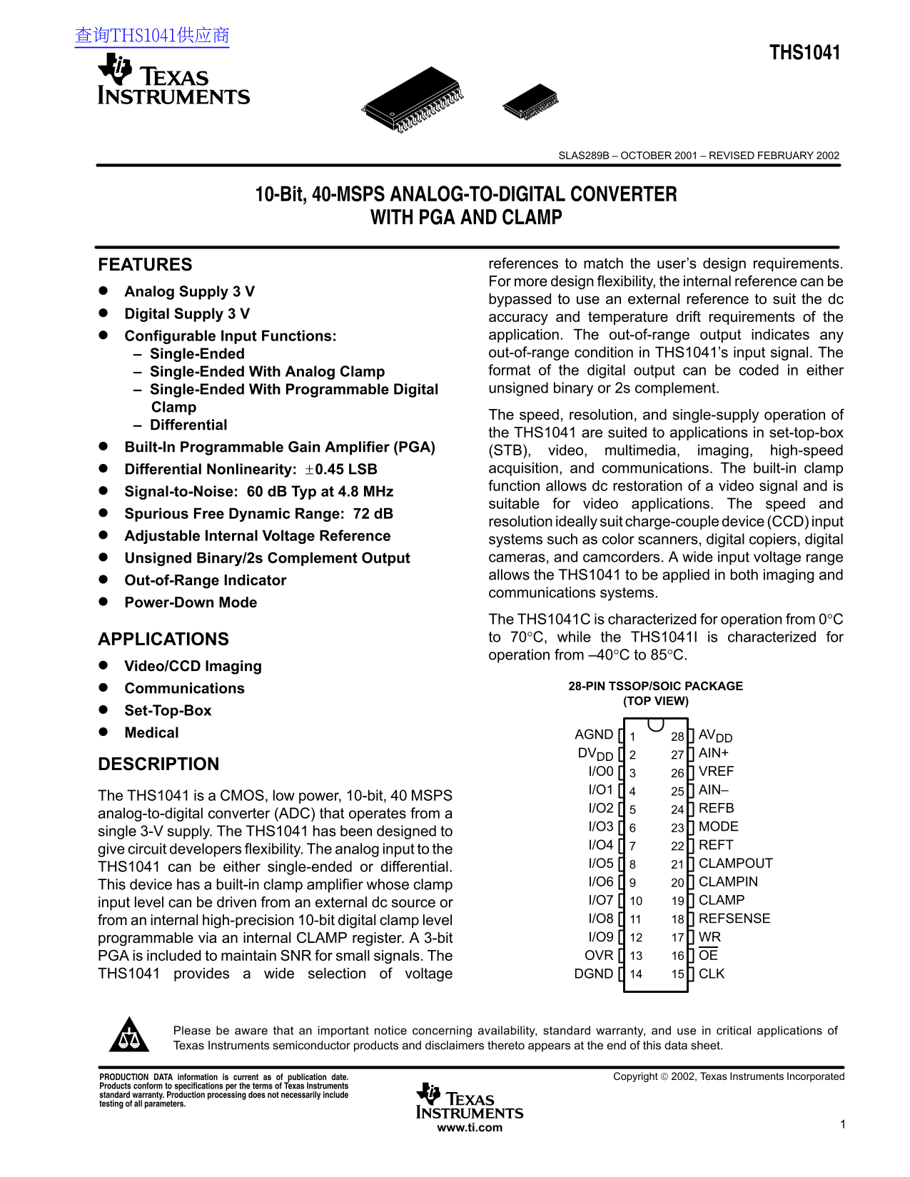
Communications 28-PIN TSSOP/SOIC PACKAGE

(TOP VIEW)

Set-Top-Box Medical AGND AVDD

DVDD AIN+

DESCRIPTION

I/O0 VREF I/O1 AIN–

The THS1041 is a CMOS, low power, 10-bit, 40 MSPS

I/O2 REFB

analog-to-digital converter (ADC) that operates from a

I/O3 MODE

single 3-V supply. The THS1041 has been designed to

I/O4 REFT

give circuit developers flexibility. The analog input to the

I/O5 CLAMPOUT

THS1041 can be either single-ended or differential.

This device has a built-in clamp amplifier whose clamp I/O6 CLAMPIN input level can be driven from an external dc source or I/O7 CLAMP from an internal high-precision 10-bit digital clamp level I/O8 REFSENSE programmable via an internal CLAMP register. A 3-bit I/O9 WR PGA is included to maintain SNR for small signals. The OVR OE

THS1041 provides a wide selection of voltage DGND CLK

Please be aware that an important notice concerning availability, standard warranty, and use in critical applications of Texas Instruments semiconductor products and disclaimers thereto appears at the end of this data sheet.

PRODUCTION DATA information is current as of publication date. Copyright  2002, Texas Instruments Incorporated

Products conform to specifications per the terms of Texas Instruments standard warranty. Production processing does not necessarily include testing of all parameters.

1www.ti.com

Page Summary Contents For Texas Instruments THS1041 Data Sheet / Manual

Page 1 查询THS1041供应商 THS1041 SLAS289B – OCTOBER 2001 – REVISED FEBRUARY 2002 10-Bit, 40-MSPS ANALOG-TO-DIGITAL CONVERTER WITH PGA AND CLAMP FEATURES references to match the user’s design requirements. For mor...
Page 2 THS1041 SLAS289B – OCTOBER 2001 – REVISED FEBRUARY 2002 AVAILABLE OPTIONS PACKAGED DEVICES 28-TSSOP (PW) 28-SOIC (DW) 0°C to 70°C THS1041CPW THS1041CDW –40°C to 85°C THS1041IPW THS1041IDW functional b...
Page 3 THS1041 SLAS289B – OCTOBER 2001 – REVISED FEBRUARY 2002 Terminal Functions TERMINAL I/O DESCRIPTION NAME NO. AGND Analog ground AIN+ Positive analog input AIN– Negative analog input AVDD Analog supply...
Page 4 THS1041 SLAS289B – OCTOBER 2001 – REVISED FEBRUARY 2002 absolute maximum ratings over operating free-air temperature (unless otherwise noted)† Supply voltage range: AVDD to AGND, DVDD to DGND –0.3 V t...
Page 5 THS1041 SLAS289B – OCTOBER 2001 – REVISED FEBRUARY 2002 electrical characteristics over recommended operating conditions, AVDD = 3 V, DVDD = 3 V, fs = 40 MSPS/50% duty cycle, MODE = AVDD (internal ref...
Page 6 THS1041 SLAS289B – OCTOBER 2001 – REVISED FEBRUARY 2002 electrical characteristics over recommended operating conditions, AVDD = 3 V, DVDD = 3 V, fs = 40 MSPS/50% duty cycle, MODE = AVDD (internal ref...
Page 7 THS1041 SLAS289B – OCTOBER 2001 – REVISED FEBRUARY 2002 electrical characteristics over recommended operating conditions, AVDD = 3 V, DVDD = 3 V, fs = 40 MSPS/50% duty cycle, MODE = AVDD (internal ref...
Page 8 THS1041 SLAS289B – OCTOBER 2001 – REVISED FEBRUARY 2002 PARAMETER MEASUREMENT INFORMATION OE See Note A tw(WP) td(OEW) td(WOE) thtd(DZ) td(DEN)tsu Hi-Z Hi-Z I/O Input Output Output NOTE A: All timing ...
Page 9 THS1041 SLAS289B – OCTOBER 2001 – REVISED FEBRUARY 2002 TYPICAL CHARACTERISTICS DIFFERENTIAL NONLINEARITY IN In te ra l N lin ea ri ty IN In te ra l N lin ea ri ty INPUT CODE if fe re ti al lin ea ri ...
Page 10 THS1041 ig al -t -N is at io ta l H ar ic is to rt io SLAS289B – OCTOBER 2001 – REVISED FEBRUARY 2002 TYPICAL CHARACTERISTICS TOTAL HARMONIC DISTORTION TOTAL HARMONIC DISTORTION vs vs INPUT FREQUENCY ...
Page 11 THS1041 SLAS289B – OCTOBER 2001 – REVISED FEBRUARY 2002 ta l H ar ic is to rt io IN ig al -t -N is lu is to rt io TYPICAL CHARACTERISTICS SIGNAL-TO-NOISE PLUS DISTORTION TOTAL HARMONIC DISTORTION vs v...
Page 12 THS1041 ig al -t -N is at io ri re yn am ic an SLAS289B – OCTOBER 2001 – REVISED FEBRUARY 2002 TYPICAL CHARACTERISTICS SPURIOUS FREE DYNAMIC RANGE TOTAL HARMONIC DISTORTION vs vs SUPPLY VOLTAGE SUPPLY...
Page 13 THS1041 SLAS289B – OCTOBER 2001 – REVISED FEBRUARY 2002 ef er en ce lt ag rr TYPICAL CHARACTERISTICS fi = 10 MHz at –0.5 d BFS, CLK = 40 MSPS –20 Input = 2 V Differential –40 Frequency – MHz Figure 18...
Page 14 THS1041 lit ef t, ef ef er en ce lt ag SLAS289B – OCTOBER 2001 – REVISED FEBRUARY 2002 TYPICAL CHARACTERISTICS POWER DISSIPATION POWER-UP TIME FOR INTERNAL vs REFERENCE VOLTAGE FROM STANDBY SAMPLE RAT...
Page 15 THS1041 SLAS289B – OCTOBER 2001 – REVISED FEBRUARY 2002 PRINCIPLES OF OPERATION functional overview Refer to functional block diagram. A single-ended, sample rate clock is required at pin CLK for devi...
Page 16 THS1041 SLAS289B – OCTOBER 2001 – REVISED FEBRUARY 2002 PRINCIPLES OF OPERATION sample-and-hold Differential input signal sources can be connected directly to the AIN+ and AIN– pins using either dc- o...
Page 17 THS1041 SLAS289B – OCTOBER 2001 – REVISED FEBRUARY 2002 PRINCIPLES OF OPERATION ADC reference generation The THS1041 ADC references REFT and REFB can be driven from external (off-chip) sources or from...
Page 18 THS1041 SLAS289B – OCTOBER 2001 – REVISED FEBRUARY 2002 PRINCIPLES OF OPERATION internal reference mode (MODE = AVDD or AVDD/2) AVDD + VREF Sample ADC AIN+ X1 and Core PGA AIN– X–1 Hold AVDD – VREF VR...
Page 19 THS1041 SLAS289B – OCTOBER 2001 – REVISED FEBRUARY 2002 PRINCIPLES OF OPERATION internal reference mode (MODE = AVDD or AVDD/2) (continued) AVDD or +FS AIN+ AIN+ MODE –FS +FS AIN– AIN– REFSENSE REFT V...
Page 20 THS1041 SLAS289B – OCTOBER 2001 – REVISED FEBRUARY 2002 PRINCIPLES OF OPERATION onboard reference generator configuration The internal bandgap reference A1 can provide a supply-voltage-independent and...
Page 21 THS1041 SLAS289B – OCTOBER 2001 – REVISED FEBRUARY 2002 PRINCIPLES OF OPERATION onboard reference generator configuration (continued) ADC References Buffer A2 MODE = AVDD or AVDD VREF = 1 V REFSENSE F...
Page 22 THS1041 SLAS289B – OCTOBER 2001 – REVISED FEBRUARY 2002 PRINCIPLES OF OPERATION onboard reference generator configuration (continued) ADC References Buffer A2 MODE = AVDD or AVDD VREF = External REFSE...
Page 23 THS1041 SLAS289B – OCTOBER 2001 – REVISED FEBRUARY 2002 PRINCIPLES OF OPERATION operating configuration examples (continued) Figure 35 shows a configuration using the internal ADC references for digit...
Page 24 THS1041 SLAS289B – OCTOBER 2001 – REVISED FEBRUARY 2002 PRINCIPLES OF OPERATION operating configuration examples (continued) Figure 37 shows a configuration using external ADC references for digitizin...
Page 25 THS1041 SLAS289B – OCTOBER 2001 – REVISED FEBRUARY 2002 PRINCIPLES OF OPERATION clamp operation (continued) Black Line Sync Level Video at AIN CLAMP Figure 39. Example Waveforms for Line-Clamping to a...
Page 26 THS1041 SLAS289B – OCTOBER 2001 – REVISED FEBRUARY 2002 PRINCIPLES OF OPERATION power management In power-sensitive applications (such as battery-powered systems) where the THS1041 ADC is not required...
Page 27 THS1041 SLAS289B – OCTOBER 2001 – REVISED FEBRUARY 2002 PRINCIPLES OF OPERATION digital control registers The THS1041 contains two clamp registers and a control register for user programming of THS104...
Page 28 THS1041 SLAS289B – OCTOBER 2001 – REVISED FEBRUARY 2002 APPLICATION INFORMATION driving the THS1041 analog inputs driving the clock input Obtaining good performance from the THS1041 requires care when...
Page 29 THS1041 SLAS289B – OCTOBER 2001 – REVISED FEBRUARY 2002 APPLICATION INFORMATION AVDD R2 = 1/CS f CLK IIN C1 8 p F VCM = AIN+/AIN– Common Mode Voltage Figure 43. Equivalent Circuit for the AIN Switched...
Page 30 THS1041 SLAS289B – OCTOBER 2001 – REVISED FEBRUARY 2002 APPLICATION INFORMATION driving the VREF pin (continued) Note that the maximum current may be up to 30% higher. The user should ensure that VREF...
Page 31 THS1041 SLAS289B – OCTOBER 2001 – REVISED FEBRUARY 2002 APPLICATION INFORMATION initial clamp acquisition time (continued) Initial acquisition can be performed in two ways: Pulsing the CLAMP pin as in...
Page 32 THS1041 SLAS289B – OCTOBER 2001 – REVISED FEBRUARY 2002 APPLICATION INFORMATION steady-state clamp voltage error (continued) V(Clamp) VDROOP = ∆VAIN tc td Figure 47. Approximate Waveforms at AIN Durin...
Page 33 THS1041 SLAS289B – OCTOBER 2001 – REVISED FEBRUARY 2002 APPLICATION INFORMATION CLAMPOUT decoupling (when used as dc bias source) When using CLAMPOUT as a dc biasing reference (e.g., MODE = AVDD), the...
Page 34 THS1041 SLAS289B – OCTOBER 2001 – REVISED FEBRUARY 2002 APPLICATION INFORMATION definitions Integral nonlinearity (INL)—Integral nonlinearity refers to the deviation of each individual code from a lin...
Page 35 THS1041 SLAS289B – OCTOBER 2001 – REVISED FEBRUARY 2002 MECHANICAL DATA DW (R-PDSO-G**) PLASTIC SMALL-OUTLINE 16 PINS SHOWN 0.299 (7,59) 0.010 (0,25) NOM Gage Plane Seating Plane 0.104 (2,65) MAX PINS...
Page 36 THS1041 SLAS289B – OCTOBER 2001 – REVISED FEBRUARY 2002 MECHANICAL DATA PW (R-PDSO-G**) PLASTIC SMALL-OUTLINE 14 PINS SHOWN 0,15 NOM Gage Plane Seating Plane 1,20 MAX 0,10 PINS ** DIM A MAX 3,10 5,10 ...
Page 37 IMPORTANT NOTICE Texas Instruments Incorporated and its subsidiaries (TI) reserve the right to make corrections, modifications, enhancements, improvements, and other changes to its products and servic...

Manual Details

Brand Texas Instruments
Pages 37
File Size 507.80 KB
Published July 12, 2026
0 views

Enter the captcha to get the download link:

captcha

Frequently Asked Questions

What temperature ranges are available for the THS1041?

The THS1041C is characterized for 0°C to 70°C, while the THS1041I supports -40°C to 85°C.

How can I use an external voltage reference instead of the internal one?

The analog supply can be bypassed by connecting the Analog Supply 3V to use an external reference source for improved accuracy and drift control.

What features help restore dc signals, such as video signals?

The device has a built-in programmable clamp amplifier that enables dc restoration capability in out-of-range conditions.

Does the THS1041 support multiple digital output formats?

Yes, it supports single-ended outputs coded either as unsigned binary or 2s complement.