Texas Instruments SN74CBTD3384C Data Sheet Manual
Summary
This high-speed, TTL-compatible FET bus switch is designed for reliable signal switching in both digital and analog systems. It features essential protections, including active undershoot clamping and integrated voltage level shifting (5V to 3.3V), ensuring robust data integrity. The associated manual provides detailed functional diagrams, comprehensive electrical specifications (including ESD/Latch-up performance), and ordering information necessary for system designers. This device is ideal for applications requiring low-impedance bidirectional data flow and efficient operation during partial power-down cycles.
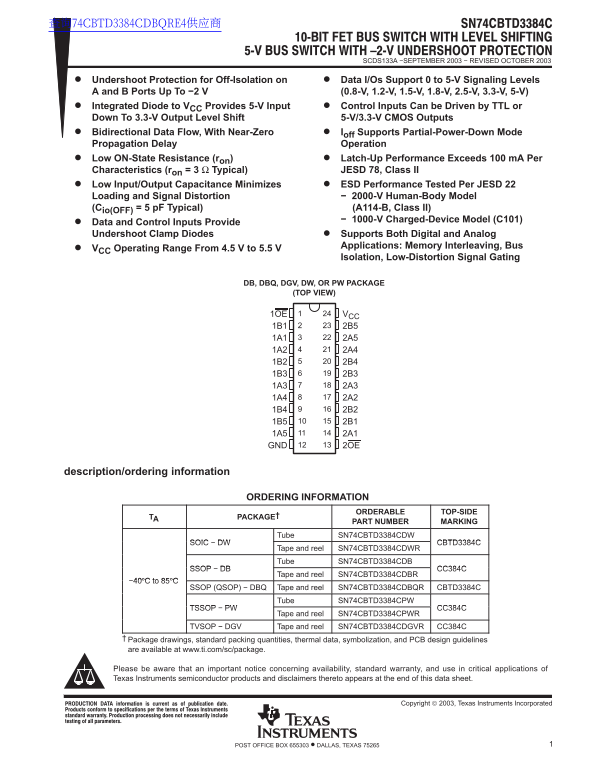
Page 1 Text Content
查询74CBTD3384CDBQRE4供应商
SCDS133A −SEPTEMBER 2003 − REVISED OCTOBER 2003
Undershoot Protection for Off-Isolation on Data I/Os Support 0 to 5-V Signaling Levels A and B Ports Up To −2 V (0.8-V, 1.2-V, 1.5-V, 1.8-V, 2.5-V, 3.3-V, 5-V) Integrated Diode to VCC Provides 5-V Input Control Inputs Can be Driven by TTL or Down To 3.3-V Output Level Shift 5-V/3.3-V CMOS Outputs Bidirectional Data Flow, With Near-Zero Ioff Supports Partial-Power-Down Mode Propagation Delay Operation Low ON-State Resistance (ron) Latch-Up Performance Exceeds 100 m A Per Characteristics (ron = 3 Ω Typical) JESD 78, Class II Low Input/Output Capacitance Minimizes ESD Performance Tested Per JESD 22 Loading and Signal Distortion − 2000-V Human-Body Model (Cio(OFF) = 5 p F Typical) (A114-B, Class II)
− 1000-V Charged-Device Model (C101)
Data and Control Inputs Provide Undershoot Clamp Diodes Supports Both Digital and Analog
Applications: Memory Interleaving, Bus
VCC Operating Range From 4.5 V to 5.5 V
Isolation, Low-Distortion Signal Gating
DB, DBQ, DGV, DW, OR PW PACKAGE
(TOP VIEW)
1OE VCC
1B1 2B5 1A1 2A5 1A2 2A4 1B2 2B4 1B3 2B3 1A3 2A3 1A4 2A2 1B4 2B2 1B5 2B1 1A5 2A1 GND 2OE
description/ordering information
ORDERING INFORMATION
ORDERABLE TOP-SIDE
TA PACKAGE†
PART NUMBER MARKING
Tube SN74CBTD3384CDW
SOIC − DW CBTD3384C
Tape and reel SN74CBTD3384CDWR Tube SN74CBTD3384CDB
SSOP − DB CC384C
Tape and reel SN74CBTD3384CDBR
−40°C to 85°C
SSOP (QSOP) − DBQ Tape and reel SN74CBTD3384CDBQR CBTD3384C
Tube SN74CBTD3384CPW
TSSOP − PW CC384C
Tape and reel SN74CBTD3384CPWR
TVSOP − DGV Tape and reel SN74CBTD3384CDGVR CC384C
Package drawings, standard packing quantities, thermal data, symbolization, and PCB design guidelines are available at www.ti.com/sc/package.
Please be aware that an important notice concerning availability, standard warranty, and use in critical applications of Texas Instruments semiconductor products and disclaimers thereto appears at the end of this data sheet.
!"#$%& " ' ()##* & %' "! +),- (%& " .%&*/ Copyright 2003, Texas Instruments Incorporated
1POST OFFICE BOX 655303 • DALLAS, TEXAS 75265
Page Summary Contents For Texas Instruments SN74CBTD3384C Data Sheet Manual
Manual Details
| Brand | Texas Instruments |
|---|---|
| Pages | 16 |
| File Size | 349.87 KB |
| Published | June 18, 2026 |
Enter the captcha to get the download link:

Frequently Asked Questions
Does this switch support multiple voltage levels?
Yes, it includes an integrated diode to provide level shifting for 5-V input down to 3.3-V output levels.
How is data flow managed between ports A and B?
When OE is low (ON), the A port connects to the B port, allowing bidirectional data flow. When open (OE high), it enters a high-impedance state.
What protection is offered against voltage dips?
The device features Active Undershoot-Protection Circuitry on both ports, protecting against undershoot up to -2 V.
Can I use this switch in partial power-down mode?
Yes, it fully supports partial-power-down applications using the $I_{OFF}$ feature, ensuring isolation and preventing damaging current backflow.