Texas Instruments SN74CB3Q3251 Data Sheet Manual
Summary
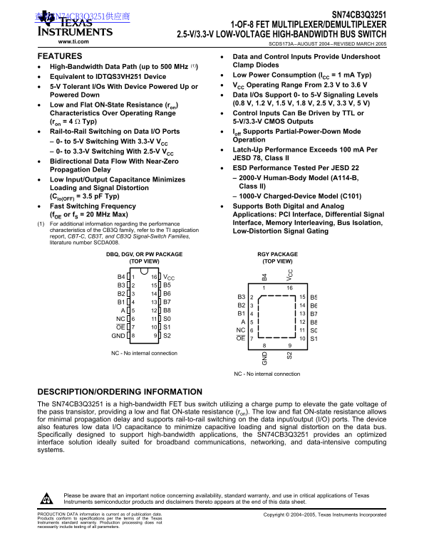
The SN74CB3Q3251 is a 1-of-8 FET multiplexer/demultiplexer from Texas Instruments for 2.5V/3.3V applications. It features 500MHz bandwidth, 4Ohm on-resistance, 5V tolerant I/Os, undershoot clamp diodes, near-zero propagation delay, and partial-power-down mode. Available in TSSOP, SSOP, and TVSOP packages, it supports digital and analog applications including PCI interface, differential signaling, memory interleaving, bus isolation, and signal gating. It targets digital system designers in computing and communications requiring high-bandwidth signal routing.
Page 1 Text Content
查询SN74CB3Q3251供应商 SN74CB3Q3251
1-OF-8 FET MULTIPLEXER/DEMULTIPLEXER
2.5-V/3.3-V LOW-VOLTAGE HIGH-BANDWIDTH BUS SWITCH
www.ti.com
SCDS173A–AUGUST 2004–REVISED MARCH
FEATURES Data and Control Inputs Provide Undershoot
(1)) Clamp Diodes•
High-Bandwidth Data Path (up to MHz
Low Power Consumption (ICC m A Typ)•
Equivalent to IDTQS3VH251 Device
VCC Operating Range From 2.3 to 3.6 V•
5-V Tolerant I/Os With Device Powered Up or
Powered Down Data I/Os Support 0- to 5-V Signaling Levels
Low and Flat ON-State Resistance (ron)
Characteristics Over Operating Range Control Inputs Can Be Driven by TTL or
(ron Typ) 5-V/3.3-V CMOS Outputs
Rail-to-Rail Switching on Data I/O Ports Ioff Supports Partial-Power-Down Mode
Operation–
0- to 5-V Switching With 3.3-V VCC
Latch-Up Performance Exceeds m A Per–
0- to 3.3-V Switching With 2.5-V VCC
JESD 78, Class II•
Bidirectional Data Flow With Near-Zero
ESD Performance Tested Per JESD 22Propagation
Delay
2000-V Human-Body Model (A114-B,•
Low Input/Output Capacitance Minimizes
Class II)Loading
and Signal Distortion
(Cio(OFF) 3.5 p F Typ) 1000-V Charged-Device Model (C101)
Fast Switching Frequency Supports Both Digital and Analog
(f OE or f S MHz Max) Applications: PCI Interface, Differential Signal
For additional information regarding the performance Interface, Memory Interleaving, Bus Isolation,(1)
characteristics of the CB3Q family, refer to the TI application
Low-Distortion Signal Gating
report, CBT-C, CB3T, and CB3Q Signal-Switch Families,
literature number SCDA008.
DBQ, DGV, OR PW PACKAGE RGY PACKAGE
(TOP VIEW) (TOP VIEW)
B4 VCC B3 B5 B2 B6
NC S0
OE S1
NC S0
GND S2
OE S1
NC - No internal connection
NC - No internal connection
DESCRIPTION/ORDERING INFORMATION
The SN74CB3Q3251 is high-bandwidth FET bus switch utilizing charge pump to elevate the gate voltage of
the pass transistor, providing low and flat ON-state resistance (ron). The low and flat ON-state resistance allows
for minimal propagation delay and supports rail-to-rail switching on the data input/output (I/O) ports. The device
also features low data I/O capacitance to minimize capacitive loading and signal distortion on the data bus.
Specifically designed to support high-bandwidth applications, the SN74CB3Q3251 provides an optimized
interface solution ideally suited for broadband communications, networking, and data-intensive computing
systems.
Please be aware that an important notice concerning availability, standard warranty, and use in critical applications of Texas
Instruments semiconductor products and disclaimers thereto appears at the end of this data sheet.
PRODUCTION DATA information is current as of publication date. Copyright 2004–2005, Texas Instruments Incorporated
Products conform to specifications per the terms of the Texas
Instruments standard warranty. Production processing does not
necessarily include testing of all parameters.
Page Summary Contents For Texas Instruments SN74CB3Q3251 Data Sheet Manual
Manual Details
| Brand | Texas Instruments |
|---|---|
| Pages | 14 |
| File Size | 376.98 KB |
| Published | June 16, 2026 |
Enter the captcha to get the download link:

Frequently Asked Questions
What is the operating voltage range of SN74CB3Q3251?
It operates from 2.3 V to 3.6 V.
How to enable the multiplexer/demultiplexer?
Set OE low to enable bidirectional data flow between A and B ports.
What is the max data path bandwidth?
The high-bandwidth data path supports up to 500 MHz.
Is the device 5V tolerant?
Yes, I/Os are 5V tolerant with device powered up or down.