Texas Instruments SN54F244, SN74F244 User's Manual
Summary
These octal buffers and line drivers are critical components for improving the performance and density of digital circuits, designed to drive bus lines or buffer memory address signals using high-reliability 3-state outputs. This technical guide provides comprehensive specifications for both SN54F244 and SN74F244 series, detailing operational parameters, multiple package options (SOIC, SSOP, DIP), and diverse temperature ranges. It is the essential resource for electronics engineers building robust data handling systems in logic and memory applications.
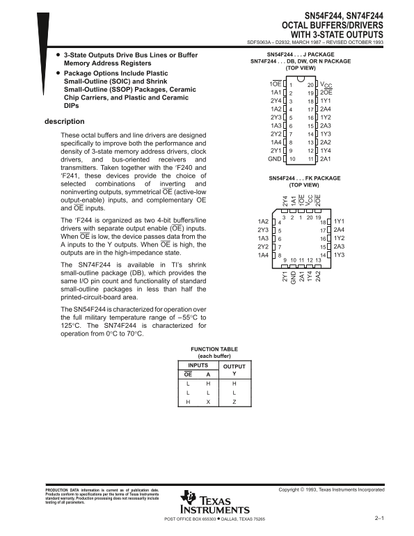
Page 1 Text Content
SN54F244, SN74F244 OCTAL BUFFERS/DRIVERS WITH 3-STATE OUTPUTS
SDFS063A – D2932, MARCH 1987 – REVISED OCTOBER 1993
3-State Outputs Drive Bus Lines or Buffer SN54F244 J PACKAGE SN74F244 DB, DW, OR N PACKAGE
Memory Address Registers
(TOP VIEW)
Package Options Include Plastic Small-Outline (SOIC) and Shrink
1OE VCC
Small-Outline (SSOP) Packages, Ceramic
1A1 2OE
Chip Carriers, and Plastic and Ceramic
description
1A3 2A3 These octal buffers and line drivers are designed 2Y2 1Y3 specifically to improve both the performance and 1A4 2A2 density of 3-state memory address drivers, clock 2Y1 1Y4 drivers, and bus-oriented receivers and GND 2A1
transmitters. Taken together with the ′F240 and ′F241, these devices provide the choice of
SN54F244 FK PACKAGE
selected combinations of inverting and (TOP VIEW) noninverting outputs, symmetrical OE (active-low output-enable) inputs, and complementary OE and OE inputs. The ′F244 is organized as two 4-bit buffers/line 1A2 1Y1 drivers with separate output enable (OE) inputs. 2Y3 2A4 When OE is low, the device passes data from the 1Y2
A inputs to the Y outputs. When OE is high, the
outputs are in the high-impedance state.
The SN74F244 is available in TI’s shrink small-outline package (DB), which provides the same I/O pin count and functionality of standard
small-outline packages in less than half the
printed-circuit-board area.
The SN54F244 is characterized for operation over 1Y the full military temperature range of –55°C to 2A 2O 125°C. The SN74F244 is characterized for operation from 0°C to 70°C.
FUNCTION TABLE (each buffer) INPUTS OUTPUT OE
PRODUCTION DATA information is current as of publication date. Copyright 1993, Texas Instruments Incorporated
Products conform to specifications per the terms of Texas Instruments standard warranty. Production processing does not necessarily include testing of all parameters.
2–1POST OFFICE BOX 655303 • DALLAS, TEXAS 75265
Page Summary Contents For Texas Instruments SN54F244, SN74F244 User's Manual
Manual Details
| Brand | Texas Instruments |
|---|---|
| Pages | 15 |
| File Size | 474.20 KB |
| Published | June 15, 2026 |
Enter the captcha to get the download link:

Frequently Asked Questions
What do the octal buffers provide?
They are designed to improve the performance and density of 3-state memory address drivers, clock drivers, and bus receivers/transmitters.
How does the SN74F244 operate using Output Enable (OE)?
When OE is low, the device passes data from the A inputs to the Y outputs. When OE is high, the outputs are in a high-impedance state.
What is the operating temperature range for each variant?
The SN54F244 supports –55°C to 125°C, while the SN74F244 operates from 0°C to 70°C.
What are the operational current limits of the different parts?
Operating output currents range from 96 mA for the SN54F244 to 128 mA for the SN74F244 in a low state.