Texas Instruments CDCV304 Data Sheet/Manual
Summary
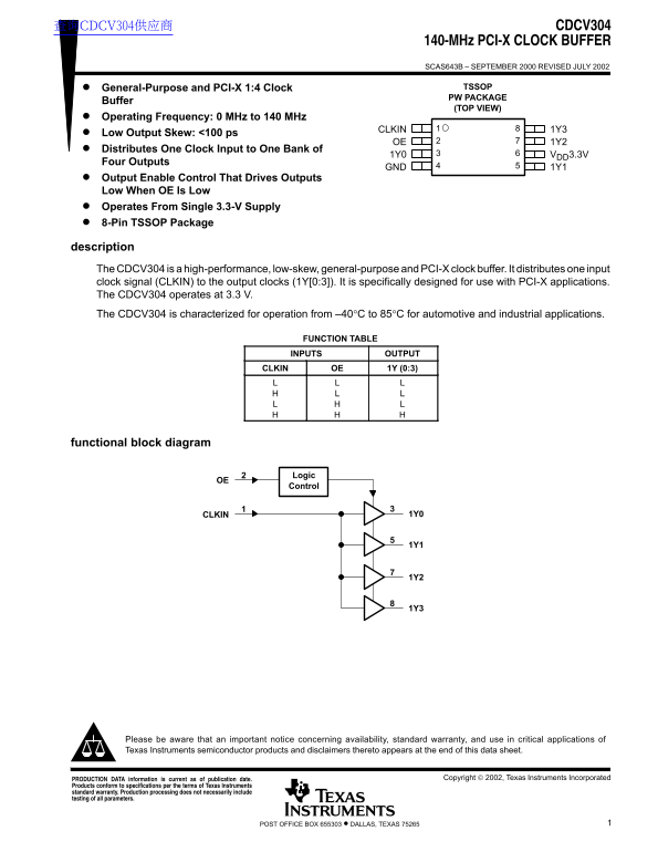
Texas Instruments CDCV304 140-MHz PCI-X clock buffer in 8-pin TSSOP distributing one clock input to four outputs with less than 100ps skew. Operates from 3.3V with output enable control, characterized for -40 to 85 degrees Celsius. For digital designers implementing clock trees in PCI-X interfaces and microprocessor systems.
Page 1 Text Content
查询CDCV304供应商 CDCV304
140-MHz PCI-X CLOCK BUFFER SCAS643B – SEPTEMBER 2000 REVISED JULY 2002 General-Purpose and PCI-X 1:4 Clock TSSOP PW PACKAGE
Buffer
(TOP VIEW)
Operating Frequency: 0 MHz to 140 MHz
CLKIN 1Y3
Low Output Skew: <100 ps
OE 1Y2
Distributes One Clock Input to One Bank of
1Y0 VDD3.3V
Four Outputs
GND 1Y1
Output Enable Control That Drives Outputs Low When OE Is Low Operates From Single 3.3-V Supply 8-Pin TSSOP Package
description The CDCV304 is a high-performance, low-skew, general-purpose and PCI-X clock buffer. It distributes one input clock signal (CLKIN) to the output clocks (1Y[0:3]). It is specifically designed for use with PCI-X applications. The CDCV304 operates at 3.3 V. The CDCV304 is characterized for operation from –40°C to 85°C for automotive and industrial applications.
FUNCTION TABLE INPUTS OUTPUT
CLKIN OE 1Y (0:3)
functional block diagram
Logic
Control
CLKIN 1Y0
Please be aware that an important notice concerning availability, standard warranty, and use in critical applications of Texas Instruments semiconductor products and disclaimers thereto appears at the end of this data sheet.
Copyright 2002, Texas Instruments Incorporated PRODUCTION DATA information is current as of publication date.
Products conform to specifications per the terms of Texas Instruments standard warranty. Production processing does not necessarily include testing of all parameters.
1POST OFFICE BOX 655303 • DALLAS, TEXAS 75265
Page Summary Contents For Texas Instruments CDCV304 Data Sheet/Manual
Manual Details
| Brand | Texas Instruments |
|---|---|
| Pages | 8 |
| File Size | 107.10 KB |
| Published | June 17, 2026 |
Enter the captcha to get the download link:

Frequently Asked Questions
What is the operating frequency range of CDCV304?
It operates from 0 MHz to 140 MHz.
What supply voltage does CDCV304 require?
It operates from a single 3.3 V supply, 3.6 V max.
How does the OE pin control the outputs?
When OE is low, outputs are driven low; high OE enables normal output.
What is the output skew specification?
The low output skew is less than 100 ps.