Texas Instruments CDCR61A Data Sheet/Manual
Summary
This technical manual provides comprehensive specifications for the CDCR61A, an independent crystal clock generator designed for high-speed memory interfaces using Rambus technology. It details a robust PLL-based system capable of generating differential and single-ended clock signals up to 400 MHz. The document covers functional modes (Normal/Test), power requirements, terminal functions, electrical ratings, and operational diagrams, making it an essential resource for electrical engineers designing high-speed data transfer systems requiring precise clock synchronization.
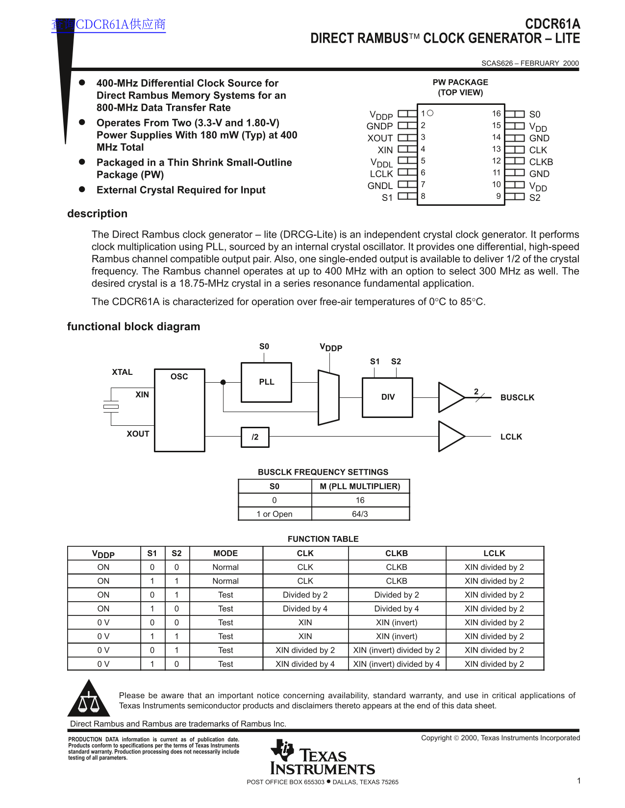
Page 1 Text Content
查询CDCR61A供应商 CDCR61A
DIRECT RAMBUS CLOCK GENERATOR – LITE
SCAS626 – FEBRUARY 2000
400-MHz Differential Clock Source for PW PACKAGE (TOP VIEW)
Direct Rambus Memory Systems for an 800-MHz Data Transfer Rate
VDDP S0
Operates From Two (3.3-V and 1.80-V)
GNDP VDD
Power Supplies With 180 m W (Typ) at 400
XOUT GND
MHz Total
XIN CLK Packaged in a Thin Shrink Small-Outline VDDL CLKB
Package (PW) LCLK GND GNDL VDD
External Crystal Required for Input
description The Direct Rambus clock generator – lite (DRCG-Lite) is an independent crystal clock generator. It performs clock multiplication using PLL, sourced by an internal crystal oscillator. It provides one differential, high-speed Rambus channel compatible output pair. Also, one single-ended output is available to deliver 1/2 of the crystal frequency. The Rambus channel operates at up to 400 MHz with an option to select 300 MHz as well. The desired crystal is a 18.75-MHz crystal in a series resonance fundamental application. The CDCR61A is characterized for operation over free-air temperatures of 0°C to 85°C.
functional block diagram
S0 VDDP
DIV BUSCLK
/2 LCLK
BUSCLK FREQUENCY SETTINGS S0 M (PLL MULTIPLIER)
1 or Open 64/3
FUNCTION TABLE
VDDP S1 S2 MODE CLK CLKB LCLK
ON Normal CLK CLKB XIN divided by 2 ON Normal CLK CLKB XIN divided by 2 ON Test Divided by 2 Divided by 2 XIN divided by 2 ON Test Divided by 4 Divided by 4 XIN divided by 2 0 V Test XIN XIN (invert) XIN divided by 2 0 V Test XIN XIN (invert) XIN divided by 2 0 V Test XIN divided by 2 XIN (invert) divided by 2 XIN divided by 2 0 V Test XIN divided by 4 XIN (invert) divided by 4 XIN divided by 2
Please be aware that an important notice concerning availability, standard warranty, and use in critical applications of Texas Instruments semiconductor products and disclaimers thereto appears at the end of this data sheet.
Direct Rambus and Rambus are trademarks of Rambus Inc.
Copyright 2000, Texas Instruments Incorporated PRODUCTION DATA information is current as of publication date.
Products conform to specifications per the terms of Texas Instruments standard warranty. Production processing does not necessarily include testing of all parameters.
1POST OFFICE BOX 655303 • DALLAS, TEXAS 75265
Page Summary Contents For Texas Instruments CDCR61A Data Sheet/Manual
Manual Details
| Brand | Texas Instruments |
|---|---|
| Pages | 10 |
| File Size | 135.32 KB |
| Published | June 22, 2026 |
Enter the captcha to get the download link:

Frequently Asked Questions
What crystal frequency is required for this clock generator?
A desired external crystal is an 18.75-MHz crystal.ቸው
What is the maximum operating speed of the Rambus channel?
The Rambus channel operates at up to 400 MHz, with an option to select 300 MHz.
How can I obtain a signal other than the main Rambus clock output?
It provides one single-ended output (LCLK) which delivers 1/2 of the crystal frequency.
What is the recommended operating temperature range for the CDCR61A?
The device is characterized for operation over free-air temperatures of 0°C to 85°C.