# A B C D E F G H I J K L M N O P Q R S T U V W X Y Z

Texas Instruments - ADS8343 Data Sheet manual specifications guide

Summary

This datasheet describes the Texas Instruments ADS8343, a 16-bit 4-channel sampling analog-to-digital converter with synchronous serial interface, pin-compatible with the ADS7841 and ADS8341. Operating from a single 2.7V to 5V supply, it achieves up to 100kHz conversion rate with 86dB SINAD while dissipating only 8mW at 100kHz and 5V. The reference voltage is adjustable from 500mV to VCC/2, providing a corresponding bipolar input range of ±VREF. A shutdown mode reduces power to under 15µW. The d
📄 Preview 📖 Table of Contents Contents PAGE OF 20

Page 1 Text Content

ADS8343

ADS8343

SBAS183C – JANUARY 2001 – REVISED APRIL 2003

16-Bit, 4-Channel Serial Output Sampling ANALOG-TO-DIGITAL CONVERTER

FEATURES DESCRIPTION

BIPOLAR INPUT RANGE

The ADS8343 is a 4-channel, 16-bit sampling Analog-to- PIN-FOR-PIN COMPATIBLE WITH THE Digital (A/D) converter with a synchronous serial interface. ADS7841 AND ADS8341 Typical power dissipation is 8m W at a 100k Hz throughput rate and a +5V supply. The reference voltage (VREF) can be

SINGLE SUPPLY: 2.7V to 5V

varied between 500m V and VCC/2, providing a corresponding

4-CHANNEL SINGLE-ENDED OR

input voltage range of ±VREF. The device includes a shut-

2-CHANNEL DIFFERENTIAL INPUT

down mode which reduces power dissipation to under 15µW. UP TO 100k Hz CONVERSION RATE The ADS8343 is ensured down to 2.7V operation. 86d B SINAD Low power, high speed, and an onboard multiplexer make the ADS8343 ideal for battery-operated systems such as

SERIAL INTERFACE

personal digital assistants, portable multi-channel data log-

SSOP-16 PACKAGE

gers, and measurement equipment. The serial interface also provides low-cost isolation for remote data acquisition. The APPLICATIONS ADS8343 is available in an SSOP-16 package and is en- sured over the –40°C to +85°C temperature range.

DATA ACQUISITION TEST AND MEASUREMENT INDUSTRIAL PROCESS CONTROL PERSONAL DIGITAL ASSISTANTS BATTERY-POWERED SYSTEMS

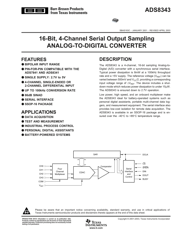
SAR DCLK

CH0 Comparator

Four Serial

Channel Interface DIN

CH2 Multiplexer and

Control

COM VREF

Please be aware that an important notice concerning availability, standard warranty, and use in critical applications of Texas Instruments semiconductor products and disclaimers thereto appears at the end of this data sheet.

PRODUCTION DATA information is current as of publication date. Copyright © 2001-2003, Texas Instruments Incorporated Products conform to specifications per the terms of Texas Instruments standard warranty. Production processing does not necessarily include testing of all parameters.

www.ti.com

Page Summary Contents For Texas Instruments - ADS8343 Data Sheet manual specifications guide

Page 1 ADS8343 ADS8343 SBAS183C – JANUARY 2001 – REVISED APRIL 2003 16-Bit, 4-Channel Serial Output Sampling ANALOG-TO-DIGITAL CONVERTER FEATURES DESCRIPTION BIPOLAR INPUT RANGE The ADS8343 is a 4-channel, 1...
Page 2 PACKAGE/ORDERING INFORMATION MAXIMUM NO INTEGRAL MISSING SPECIFIED LINEARITY CODES PACKAGE TEMPERATURE ORDERING TRANSPORT PRODUCT ERROR (LSB) ERROR (LSB) PACKAGE-LEAD DESIGNATOR(1) RANGE NUMBER MEDIA,...
Page 3 ELECTRICAL CHARACTERISTICS: +5V At TA = –40°C to +85°C, +VCC = +5V, VREF = +2.5V, f SAMPLE = 100k Hz, and f CLK = 24 • f SAMPLE = 2.4MHz, unless otherwise noted. ADS8343E ADS8343EB PARAMETER CONDITION...
Page 4 ELECTRICAL CHARACTERISTICS: +2.7V At TA = –40°C to +85°C, +VCC = +2.7V, VREF = +1.25V, f SAMPLE = 100k Hz, and f CLK = 24 • f SAMPLE = 2.4MHz, unless otherwise noted. ADS8343E ADS8343EB PARAMETER COND...
Page 5 TYPICAL CHARACTERISTICS: +5V At TA = +25°C, +VCC = +5V, VREF = +2.5V, f SAMPLE = 100k Hz, and f CLK = 24 • f SAMPLE = 2.4MHz, unless otherwise noted. pl itu de d B FREQUENCY SPECTRUM ffe ct iv um be o...
Page 6 TYPICAL CHARACTERISTICS: +5V (Cont.) At TA = +25°C, +VCC = +5V, VREF = +2.5V, f SAMPLE = 100k Hz, and f CLK = 24 • f SAMPLE = 2.4MHz, unless otherwise noted. el ta fr om 5° LS s) up pl ur re nt IL LS ...
Page 7 TYPICAL CHARACTERISTICS: +5V (Cont.) At TA = +25°C, +VCC = +5V, VREF = +2.5V, f SAMPLE = 100k Hz, and f CLK = 24 • f SAMPLE = 2.4MHz, unless otherwise noted. pl itu de d B nd WORST CASE CHANNEL-TO-CHA...
Page 8 TYPICAL CHARACTERISTICS: +2.7V (Cont.) ffe ct iv um be of its At TA = +25°C, +VCC = +2.7V, VREF = +1.25V, f SAMPLE = 100k Hz, and f CLK = 24 • f SAMPLE = 2.4MHz, unless otherwise noted. up pl ur re nt...
Page 9 TYPICAL CHARACTERISTICS: +2.7V (Cont.) At TA = +25°C, +VCC = +2.7V, VREF = +1.25V, f SAMPLE = 100k Hz, and f CLK = 24 • f SAMPLE = 2.4MHz, unless otherwise noted. ai at ch LS s) up pl ur re nt WORST-C...
Page 10 TYPICAL CHARACTERISTICS: +2.7V (Cont.) At TA = +25°C, +VCC = +2.7V, VREF = +1.25V, f SAMPLE = 100k Hz, and f CLK = 24 • f SAMPLE = 2.4MHz, unless otherwise noted. SUPPLY CURRENT vs SAMPLING FREQUENCY ...
Page 11 When the input is single-ended, the COM input is held at a In each case, care should be taken to ensure that the output fixed voltage. The CHX input swings around the same impedance of the sources dri...
Page 12 size, as the reference voltage is reduced. For example, if the converter enters the conversion mode. At this point, the input offset of a given converter is 2LSBs with a 2.5V reference, sample-and-hol...
Page 13 The SGL/DIF bit controls the multiplexer input mode: either ADS8343 can switch to the new mode. The extra cycle is single-ended (HIGH) or differential (LOW). In single-ended required because the PD0 a...
Page 14 The other method is shown in Figure 8, which uses 32 clock SYMBOL DESCRIPTION MIN TYP MAX UNITS cycles per conversion; the last seven clock cycles simply t ACQ Acquisition Time 1.5 µs shift out zeros ...
Page 15 DATA FORMAT If DCLK is active and CS is LOW while the ADS8343 is in auto power-down mode, the device will continue to dissipate The output data from the ADS8343 is in Binary Two’s some power in the di...
Page 16 NOISE AVERAGING The noise floor of the ADS8343 itself is extremely low, as can The noise of the A/D converter can be compensated by be seen from Figures 12 and 13, and is much lower than averaging the...
Page 17 PACKAGE DRAWING DBQ (R-PDSO-G**) PLASTIC SMALL-OUTLINE 24 PINS SHOWN 0.008 (0,20) NOM Gage Plane 0.069 (1,75) MAX Seating Plane PINS ** DIM A MAX A MIN NOTES: A. All linear dimensions are in inches (m...
Page 18 PACKAGE OPTION ADDENDUM www.ti.com 18-Jul-2006 PACKAGING INFORMATION Orderable Device Status Package Package Pins Package Eco Plan Lead/Ball Finish MSL Peak Temp Type Drawing Qty ADS8343E ACTIVE SSOP/...
Page 20 IMPORTANT NOTICE Texas Instruments Incorporated and its subsidiaries (TI) reserve the right to make corrections, modifications, enhancements, improvements, and other changes to its products and servic...

Manual Details

Brand Texas Instruments
Pages 20
File Size 530.76 KB
Published June 19, 2026
5 views

Enter the captcha to get the download link:

captcha

Frequently Asked Questions

What is the operating temperature range for the ADS8343?

The device operates in a range from -40°C to +85°C.

Does the ADS8343 have a low-power shutdown mode?

Yes, setting SHDN LOW puts the device into a very low power shutdown mode, reducing power dissipation to under 15μW.

What is the maximum conversion rate?

The device supports up to a 100kHz conversion rate.

How can this converter be used for battery-powered systems?

Its low power consumption and high speed make it ideal for battery-operated systems, such as personal digital assistants.