# A B C D E F G H I J K L M N O P Q R S T U V W X Y Z

Texas Instruments THS3120, THS3121 Specifications Data Sheet User Manual

Summary

This is the technical datasheet for the Texas Instruments THS3120 and THS3121 low-noise, high-output drive, current-feedback operational amplifiers. These amplifiers operate over a wide supply range of ±5V to ±15V with 475mA output current drive, 1700V/µs slew rate, and 120MHz bandwidth. The THS3120 features a power-down mode for power saving. Applications include video distribution, power FET drivers, pin drivers, and capacitive load drivers. Available in 8-pin SOIC and MSOP packages with PowerPAD. Target users are analog circuit designers and electronics engineers working on high-performance signal processing applications.
📄 Preview PAGE OF 29

Page 1 Text Content

查询THS3120供应商

THS3120, THS3121

if fe re ti al ai

www.ti.com

SLOS420A–SEPTEMBER 2003–REVISED NOVEMBER

LOW-NOISE, HIGH-OUTPUT DRIVE, CURRENT-FEEDBACK,

OPERATIONAL AMPLIFIERS

FEATURES DESCRIPTION

Low Noise

The THS3120 and THS3121 are low-noise,

p A/√Hz Noninverting Current Noise high-voltage, high output current drive, current-–

feedback amplifiers designed to operate over wide–

p A/√Hz Inverting Current Noise

if fe re ti al as eg supply range of ±5 to ±15 for today's high

2.5 n V/√Hz Voltage Noise

performance applications.

High Output Current Drive: m A

The THS3120 offers power saving mode by provid-

High Slew Rate: V/µs (RL Ω,

ing power-down pin for reducing the 7-m A quiesc-

VO VPP) ent current of the device, when the device is not

Wide Bandwidth: MHz (G 2, RL Ω) active.•

Wide Supply Range: ±5 to ±15 These amplifiers provide well-regulated ac

performance characteristics. Most notably, the 0.1-d B•

Power-Down Feature: (THS3120 Only)

flat bandwidth is exceedingly high, reaching beyond

MHz. The unity gain bandwidth of MHz allows

APPLICATIONS

for good distortion characteristics at MHz. Coupled

Video Distribution

with high 1700-V/µs slew rate, the THS3120 and

Power FET Driver THS3121 amplifiers allow for high output voltage

Pin Driver swings at high frequencies.•

Capacitive Load Driver

The THS3120 and THS3121 are offered in 8-pin

SOIC (D), and the 8-pin MSOP (DGN) packages with

Power PAD™.

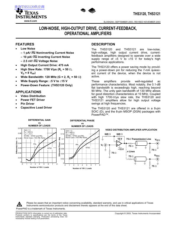
DIFFERENTIAL GAIN DIFFERENTIAL PHASE

vs vs

NUMBER OF LOADS NUMBER OF LOADS

Gain = 2, VIDEO DISTRIBUTION AMPLIFIER APPLICATION

Gain = 2,

RF = 649 Ω, RF = 649 Ω, 0.06 VS = ±15 V, 0.12 VS = ±15 V, 649 Ω 649 Ω

40 IRE − NTSC and PAL, 40 IRE − NTSC and PAL, Worst Case ±100 IRE Ramp Worst Case ±100 IRE Ramp

0.1 15 V 75-Ω Transmission Line

VO(1)

PAL 0.08

PAL VI

0.03 NTSC NTSC

−15 V 75 Ω n Lines

VO(n)

Number of 150 Ω Loads

Number of 150 Ω Loads

Please be aware that an important notice concerning availability, standard warranty, and use in critical applications of Texas

Instruments semiconductor products and disclaimers thereto appears at the end of this data sheet.

Power PAD is trademark of Texas Instruments.

PRODUCTION DATA information is current as of publication date. Copyright 2003, Texas Instruments Incorporated

Products conform to specifications per the terms of the Texas

Instruments standard warranty. Production processing does not

necessarily include testing of all parameters.

Page Summary Contents For Texas Instruments THS3120, THS3121 Specifications Data Sheet User Manual

Page 1 查询THS3120供应商 THS3120, THS3121 if fe re ti al ai www.ti.com SLOS420A–SEPTEMBER 2003–REVISED NOVEMBER LOW-NOISE, HIGH-OUTPUT DRIVE, CURRENT-FEEDBACK, OPERATIONAL AMPLIFIERS FEATURES DESCRIPTION Low Nois...
Page 2 THS3120, THS3121 www.ti.com SLOS420A–SEPTEMBER 2003–REVISED NOVEMBER This integrated circuit can be damaged by ESD. Texas Instruments recommends that all integrated circuits be handled with appropriat...
Page 3 THS3120, THS3121 www.ti.com SLOS420A–SEPTEMBER 2003–REVISED NOVEMBER RECOMMENDED OPERATING CONDITIONS MIN NOM MAX UNIT Dual supply ±5 ±15 Supply voltage Single supply Commercial Operating free-air tem...
Page 4 THS3120, THS3121 www.ti.com SLOS420A–SEPTEMBER 2003–REVISED NOVEMBER ELECTRICAL CHARACTERISTICS VS ±15 V, RF Ω,RL Ω, and (unless otherwise noted) TYP OVER TEMPERATURE PARAMETER TEST CONDITIONS 0°C to ...
Page 5 THS3120, THS3121 www.ti.com SLOS420A–SEPTEMBER 2003–REVISED NOVEMBER ELECTRICAL CHARACTERISTICS (continued) VS ±15 V, RF Ω,RL Ω, and (unless otherwise noted) TYP OVER TEMPERATURE PARAMETER TEST CONDIT...
Page 6 THS3120, THS3121 www.ti.com SLOS420A–SEPTEMBER 2003–REVISED NOVEMBER ELECTRICAL CHARACTERISTICS VS ±5 V, RF Ω, RL Ω, and (unless otherwise noted) TYP OVER TEMPERATURE PARAMETER TEST CONDITIONS 0°C to ...
Page 7 THS3120, THS3121 www.ti.com SLOS420A–SEPTEMBER 2003–REVISED NOVEMBER ELECTRICAL CHARACTERISTICS (continued) VS ±5 V, RF Ω, RL Ω, and (unless otherwise noted) TYP OVER TEMPERATURE PARAMETER TEST CONDIT...
Page 8 THS3120, THS3121 www.ti.com SLOS420A–SEPTEMBER 2003–REVISED NOVEMBER TYPICAL CHARACTERISTICS TABLE OF GRAPHS FIGURE ±15-V graphs Noninverting small signal gain frequency response 1, Inverting small si...
Page 9 THS3120, THS3121 www.ti.com SLOS420A–SEPTEMBER 2003–REVISED NOVEMBER ig al ai in ve rt in ai in ve rt in ai TYPICAL CHARACTERISTICS (±15 V) NONINVERTING SMALL SIGNAL NONINVERTING SMALL SIGNAL INVERTIN...
Page 10 THS3120, THS3121 www.ti.com SLOS420A–SEPTEMBER 2003–REVISED NOVEMBER 3r ar ic is to rt io tp t V lt ag le at sµ TYPICAL CHARACTERISTICS (±15 V) (continued) 3rd HARMONIC DISTORTION HARMONIC DISTORTION ...
Page 11 THS3120, THS3121 www.ti.com tp Vo lt ag Tr an si SLOS420A–SEPTEMBER ed an ce ai 2003–REVISED NOVEMBER tp t V lt ag TYPICAL CHARACTERISTICS (±15 V) (continued) INPUT BIAS AND OUTPUT VOLTAGE OFFSET CURR...
Page 12 THS3120, THS3121 www.ti.com SLOS420A–SEPTEMBER 2003–REVISED NOVEMBER if fe re ti al as TYPICAL CHARACTERISTICS (±15 V) (continued) CLOSED-LOOP OUTPUT POWER-DOWN QUIESCENT DIFFERENTIAL PHASE IMPEDANCE ...
Page 13 THS3120, THS3121 www.ti.com SLOS420A–SEPTEMBER 2003–REVISED NOVEMBER 3r ar ic is to rt io le at sµ in ve rt in ai TYPICAL CHARACTERISTICS (±5 V) NONINVERTING SMALL SIGNAL INVERTING SMALL SIGNAL FREQUE...
Page 14 THS3120, THS3121 www.ti.com SLOS420A–SEPTEMBER 2003–REVISED NOVEMBER tp Vo lt ag tp Vo lt ag TYPICAL CHARACTERISTICS (±5 V) (continued) INPUT BIAS AND OFFSET CURRENT NONINVERTING SMALL SIGNAL INVERTIN...
Page 15 THS3120, THS3121 www.ti.com SLOS420A–SEPTEMBER 2003–REVISED NOVEMBER APPLICATION INFORMATION Maximum Slew Rate for Repetitive Signals Current-feedback amplifiers are highly dependent on the feedback r...
Page 16 THS3120, THS3121 www.ti.com SLOS420A–SEPTEMBER 2003–REVISED NOVEMBER WIDEBAND, INVERTING OPERATION Figure shows the THS3121 in typical inverting 50 Ω Source gain configuration where the input and outp...
Page 17 THS3120, THS3121 www.ti.com SLOS420A–SEPTEMBER 2003–REVISED NOVEMBER Driving Capacitive Loads Placing small series resistor, RISO, between the amplifier’s output and the capacitive load, as shown Appl...
Page 18 THS3120, THS3121 www.ti.com SLOS420A–SEPTEMBER 2003–REVISED NOVEMBER RF VS VS VS -VS RG FB 100 Ω LOAD -VS 1 µF Figure 53. -VS -VS Figure is shown using two amplifiers in parallel to the output drive c...
Page 19 THS3120, THS3121 www.ti.com SLOS420A–SEPTEMBER 2003–REVISED NOVEMBER PRINTED-CIRCUIT BOARD LAYOUT Gain = 2 TECHNIQUES FOR OPTIMAL RF = 649 Ω PERFORMANCE er tp Im ed an ce VS = ±15 V and ±5 V Achieving...
Page 20 THS3120, THS3121 www.ti.com SLOS420A–SEPTEMBER 2003–REVISED NOVEMBER Connections to other wideband devices on the almost impossible to achieve smooth, stable board may be made with short direct traces...
Page 21 THS3120, THS3121 www.ti.com SLOS420A–SEPTEMBER 2003–REVISED NOVEMBER high thermal resistance connection that is useful for slowing the heat transfer during 0.060 soldering operations. This makes the s...
Page 22 THS3120, THS3121 www.ti.com SLOS420A–SEPTEMBER 2003–REVISED NOVEMBER Tmax TA When determining whether or not the device satisfies PDmax ax im er is si at io JA the maximum power dissipation requiremen...
Page 23 THS3120, THS3121 www.ti.com SLOS420A–SEPTEMBER 2003–REVISED NOVEMBER NOTE: The Edge number for the THS3121 is TP2GND 6445589. FB1 FB2 VS+ VS− PD J7 J5 R8A2 Vin− J6 R1 R7BR7A Z2 J4 Vin+ REF Figure 62. ...
Page 24 THS3120, THS3121 www.ti.com SLOS420A–SEPTEMBER 2003–REVISED NOVEMBER Table 2. Bill of Materials THS3120DGN and THS3121DGN EVM REFERENCE PCB MANUFACTURER'SITEM DESCRIPTION SMD SIZE DESIGNATOR QUANTITY ...
Page 25 THERMAL PAD MECHANICAL DATA www.ti.com DGN (S-PDSO-G8) THERMAL INFORMATION This Power PAD™ package incorporates an exposed thermal pad that is designed to be attached directly to an external heatsink....
Page 28 IMPORTANT NOTICE Texas Instruments Incorporated and its subsidiaries (TI) reserve the right to make corrections, modifications, enhancements, improvements, and other changes to its products and servic...
Page 29 WWW.ALLDATASHEET.COM Copyright © Each Manufacturing Company. All Datasheets cannot be modified without permission. This datasheet has been download from : www.All Data Sheet.com 100% Free Data Sheet S...

Manual Details

Brand Texas Instruments
Pages 29
File Size 858.69 KB
Published June 16, 2026
6 views

Enter the captcha to get the download link:

captcha

Frequently Asked Questions

What are the key features of the THS3120/THS3121 amplifiers?

Low noise, high output current drive (475 mA), high slew rate (1700 V/µs), wide bandwidth (120 MHz), and wide supply range (±5 V to ±15 V).

What is the main difference between THS3120 and THS3121?

Only the THS3120 has a power-down (PD) feature for reducing quiescent current.

What are the package options for these amplifiers?

They are available in 8-pin SOIC (D) and 8-pin MSOP (DGN) packages with PowerPAD.

What is the recommended supply voltage range?

The recommended dual supply range is ±5 V to ±15 V (or 10 V to 30 V single supply).