# A B C D E F G H I J K L M N O P Q R S T U V W X Y Z

Texas Instruments ADS7807 datasheet specifications user manual guide

Summary

Texas Instruments ADS7807 low-power 16-bit sampling CMOS analog-to-digital converter datasheet. The document describes SAR architecture, power-down modes, acquisition timing, input voltage ranges, and parallel/serial interface options. Target users are analog and mixed-signal design engineers developing precision measurement, data acquisition, and industrial control systems.
📄 Preview PAGE OF 24

Page 1 Text Content

ADS7807

ADS7807

ADS7807

SBAS022B – NOVEMBER 1992 – REVISED SEPTEMBER 2003

Low-Power, 16-Bit, Sampling CMOS ANALOG-to-DIGITAL CONVERTER

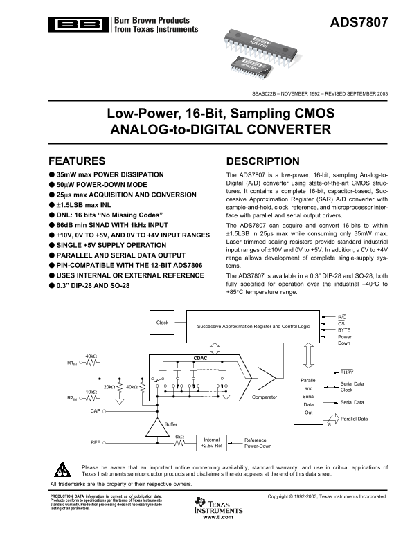
FEATURES DESCRIPTION 35m W max POWER DISSIPATION The ADS7807 is a low-power, 16-bit, sampling Analog-to-

Digital (A/D) converter using state-of-the-art CMOS struc-

50µW POWER-DOWN MODE

tures. It contains a complete 16-bit, capacitor-based, Suc-

25µs max ACQUISITION AND CONVERSION

cessive Approximation Register (SAR) A/D converter with

±1.5LSB max INL

sample-and-hold, clock, reference, and microprocessor inter-

DNL: 16 bits “No Missing Codes” face with parallel and serial output drivers. 86d B min SINAD WITH 1k Hz INPUT The ADS7807 can acquire and convert 16-bits to within

±1.5LSB in 25µs max while consuming only 35m W max.

±10V, 0V TO +5V, AND 0V TO +4V INPUT RANGES

Laser trimmed scaling resistors provide standard industrial

SINGLE +5V SUPPLY OPERATION

input ranges of ±10V and 0V to +5V. In addition, a 0V to +4V

PARALLEL AND SERIAL DATA OUTPUT

range allows development of complete single-supply sys-

PIN-COMPATIBLE WITH THE 12-BIT ADS7806 tems. USES INTERNAL OR EXTERNAL REFERENCE The ADS7807 is available in a 0.3" DIP-28 and SO-28, both

fully specified for operation over the industrial –40°C to

0.3" DIP-28 AND SO-28

+85°C temperature range.

Clock CS

Successive Approximation Register and Control Logic

BYTE Power Down

Parallel

Serial Data

Clock

R2IN Comparator Serial

Serial Data

Parallel Data

Buffer

Internal Reference

+2.5V Ref Power-Down

Please be aware that an important notice concerning availability, standard warranty, and use in critical applications of Texas Instruments semiconductor products and disclaimers thereto appears at the end of this data sheet.

All trademarks are the property of their respective owners.

PRODUCTION DATA information is current as of publication date. Copyright © 1992-2003, Texas Instruments Incorporated Products conform to specifications per the terms of Texas Instruments standard warranty. Production processing does not necessarily include testing of all parameters.

www.ti.com

Page Summary Contents For Texas Instruments ADS7807 datasheet specifications user manual guide

Page 1 ADS7807 ADS7807 ADS7807 SBAS022B – NOVEMBER 1992 – REVISED SEPTEMBER 2003 Low-Power, 16-Bit, Sampling CMOS ANALOG-to-DIGITAL CONVERTER FEATURES DESCRIPTION 35m W max POWER DISSIPATION The ADS7807 is a...
Page 2 ABSOLUTE MAXIMUM RATINGS(1) ELECTROSTATIC Analog Inputs: R1IN ±12V R2IN ±5.5V DISCHARGE SENSITIVITY CAP VANA + 0.3V to AGND2 – 0.3V REF Indefinite Short to AGND2, This integrated circuit can be damage...
Page 3 ELECTRICAL CHARACTERISTICS (Cont.) At TA = –40°C to +85°C, f S = 40k Hz, VDIG = VANA = +5V, and using internal reference and fixed resistors (see Figure 7b), unless otherwise specified. ADS7807P, U AD...
Page 4 PIN DESCRIPTIONS DIGITAL PIN # NAME I/O DESCRIPTION R1IN Analog Input. See Figure 7. AGND1 Analog Sense Ground. R2IN Analog Input. See Figure 7. CAP Reference Buffer Output. 2.2µF tantalum capacitor t...
Page 5 TYPICAL CHARACTERISTICS At TA = +25°C, f S = 40k Hz, VDIG = VANA = +5V, and using internal reference and fixed resistors (see Figure 7b), unless otherwise specified. pl itu de d B IN (d IN (d FREQUENC...
Page 6 TYPICAL CHARACTERISTICS (Cont.) er ce nt er ce nt In te rn al ef er en ce (V At TA = +25°C, f S = 40k Hz, VDIG = VANA = +5V, and using internal reference and fixed resistors (see Figure 7b), unless ot...
Page 7 BASIC OPERATION output valid data from the previous conversion on SDATA (pin 19) synchronized to 16 clock pulses output on DATACLK PARALLEL OUTPUT (pin 18). BUSY (pin 24) will go LOW and stay LOW unti...
Page 8 The ADS7807 will begin tracking the input signal at the end CS and R/C are internally OR’ed and level triggered. There of the conversion. Allowing 25µs between convert com- is not a requirement which ...
Page 9 clock pulse. As a result, data can be read on the parallel port PARALLEL OUTPUT (AFTER A CONVERSION) prior to reading the same data on the serial port, but data After conversion ‘n’ is completed and t...
Page 10 INTERNAL DATA CLOCK SYMBOL DESCRIPTION MIN TYP MAX UNITS (During a Conversion) t1 Convert Pulse Width 0.04 µs t2 Data Valid Delay after R/C LOW µs To use the internal data clock, tie EXT/INT (pin 8) L...
Page 11 it it it it (L ag ag ag ag ag ag ag ag ag FIGURE 5. Conversion and Read Timing with External Clock (EXT/INT Tied HIGH) Read after Conversion. ADS7807 SBAS022B www.ti.com
Page 12 EXTERNAL DATACLK CS t22 DATA Bit 15 (MSB) Bit 0 (LSB) Tag 0 Tag 1 TAG Tag 1 Tag 16 Tag 17 Tag 18Tag 0 FIGURE 6. Conversion and Read Timing with External Clock (EXT/INT tied HIGH) Read During a Convers...
Page 13 used for each input range (see Figure 8). The input resistor OFFSET ADJUST GAIN ADJUST divider network provides inherent over-voltage protection to INPUT RANGE RANGE (m V) RANGE (m V) at least ±5.5V f...
Page 14 ered when choosing the accuracy and drift specifications of To further analyze the effects of removing any combination of the external resistors. In most applications, 1% metal-film the external resis...
Page 15 VIN CDAC (0.3125V to 2.8125V) CDAC (0.3125V to 2.8125V) VIN CDAC (0.3125V to 2.8125V) FIGURE 9. Circuit Diagrams Showing External and Internal Resistors. tied HIGH will power-down the internal referen...
Page 16 cycle. This capacitor also provides compensation for the REFD output of the buffer. Using a capacitor any smaller than 1µF REFD HIGH will power-down the internal 2.5V reference. All can cause the outp...
Page 17 amount of charge injection due to the sampling FET switch on the ADS7807 is approximately 5% to 10% of the amount on similar A/D converters with the charge redistribution Digital-to-Analog Converter (...
Page 18 QSPI™ INTERFACING QSPI™ ADS7807 Figure 14 shows a simple interface between the ADS7807 and any QSPI equipped microcontroller. This interface as- PCS0 R/C EXT/INT sumes that the convert pulse does not ...
Page 19 DSP56000 INTERFACING similar to the QSPI interface seen in Figure 14. As mentioned in the QSPI section, the DSP56000 must be programmed to The DSP56000 serial interface has SPI compatibility mode enab...
Page 20 PACKAGE OPTION ADDENDUM www.ti.com 3-Oct-2005 PACKAGING INFORMATION Orderable Device Status Package Package Pins Package Eco Plan Lead/Ball Finish MSL Peak Temp Type Drawing Qty ADS7807P ACTIVE PDIP N...
Page 21 MECHANICAL DATA MPDI004 – OCTOBER 1994 NT (R-PDIP-T**) PLASTIC DUAL-IN-LINE PACKAGE 24 PINS SHOWN PINS ** DIM A MAX 0.280 (7,11) A MIN B MAX B MIN 0.070 (1,78) MAX 0.020 (0,51) MIN 0.200 (5,08) MAX Se...
Page 23 IMPORTANT NOTICE Texas Instruments Incorporated and its subsidiaries (TI) reserve the right to make corrections, modifications, enhancements, improvements, and other changes to its products and servic...
Page 24 WWW.ALLDATASHEET.COM Copyright © Each Manufacturing Company. All Datasheets cannot be modified without permission. This datasheet has been download from : www.All Data Sheet.com 100% Free Data Sheet S...

Manual Details

Brand Texas Instruments
Pages 24
File Size 524.22 KB
Published June 16, 2026
6 views

Enter the captcha to get the download link:

captcha

Frequently Asked Questions

What is the power consumption of the ADS7807?

Maximum power dissipation is 35mW, with a 50µW power-down mode.

What are the available input voltage ranges?

Standard input ranges are ±10V, 0V to +5V, and 0V to +4V.

What is the maximum acquisition and conversion time?

It has a maximum acquisition and conversion time of 25µs.

Is the ADS7807 compatible with the ADS7806?

Yes, it is pin-compatible with the 12-bit ADS7806.

What package options are available?

It is available in 0.3" DIP-28 and SO-28 packages.